The Importance of PCB Failure Analysis in Electronic Devices
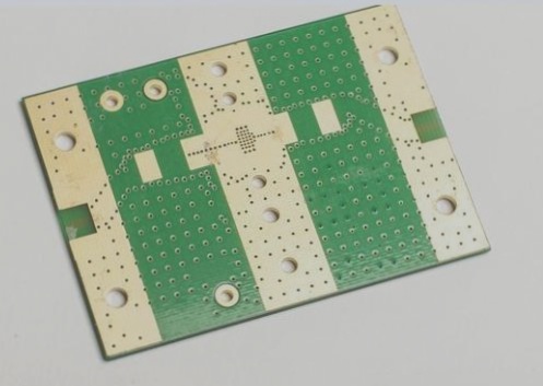
PCB boards play a crucial role in electronic information products, serving as carriers for components and facilitating circuit signal transmission. The quality and reliability of PCBs directly impact the overall performance and dependability of electronic equipment. As electronic devices continue to shrink in size and demand environmentally friendly materials, PCBs are evolving towards higher density, increased Tg, and improved sustainability.
Challenges in PCB Production and Application
Despite advancements, cost and technical constraints have led to various failure issues during PCB production and application, resulting in quality disputes. To address these challenges, thorough failure analysis is essential to identify causes and determine responsibility.
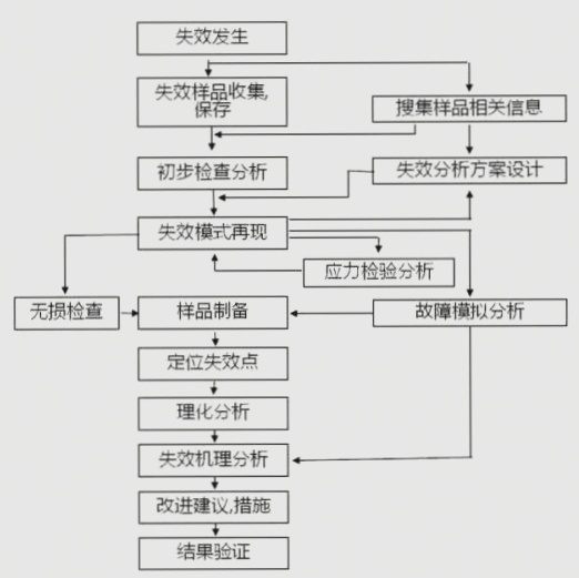
Basic Procedure of Failure Analysis
- Identifying Failure Location and Mode
- Failure Mechanism Analysis
- Failure Cause Analysis
- Test Verifications
- Compilation of Analysis
- Adhering to Analysis Principles
Failure Analysis Technology
- Optical Microscope: Used for visual inspection to identify failure parts, physical evidence, and failure modes.
- X-ray: Utilized to inspect internal defects not visible to the naked eye, particularly in high-density packaging like BGA or CSP devices.
Slicing Analysis
- Involves obtaining a cross-sectional view of the PCB through sampling, inlaying, slicing, polishing, corrosion, and observation.
- This destructive method provides detailed microstructural information that is valuable for quality improvement but results in the destruction of the sample.
Scanning Acoustic Microscope
The C-mode ultrasonic scanning acoustic microscope is primarily used for analyzing electronic packaging or assembly. It images by utilizing changes in amplitude, phase, and polarity caused by high-frequency ultrasonic reflections on discontinuous interfaces within the material. The scanning method involves gathering information in the XY plane along the Z axis. The scanning acoustic microscope can detect components, materials, and various defects within PCBs and PCBAs, including cracks, delamination, inclusions, and voids. It can also detect internal defects in solder joints if the frequency bandwidth is sufficient. Red warning colors indicate defects in scanning acoustic images. The use of plastic-packaged components in SMT processes has led to moisture reflow sensitivity issues during the transition to lead-free processes. The scanning acoustic microscope is beneficial for non-destructive flaw detection in multi-layer, high-density PCBs.
Micro-Infrared Analysis
Micro-infrared analysis combines infrared spectroscopy with microscopy to analyze the compound composition of materials based on varying infrared absorption by different materials, primarily organic matter. It helps identify trace organic pollutants visible within the field of view. Micro-infrared analysis is essential for assessing organic contaminants on welded surfaces or solder joints and analyzing causes of corrosion or poor solderability.
Scanning Electron Microscope (SEM) Analysis
The scanning electron microscope is valuable for failure analysis, particularly for topographical observation. SEMs are capable of magnifying fine structures and surface features up to hundreds of thousands of times. They help study failure mechanisms in PCB and solder joints, observe pad surfaces, metallographic structures of solder joints, intermetallic compounds, solderability, coating analysis, and tin whisker analysis. SEM produces electronic images in black and white and requires samples to be conductive.
Thermal Analysis
Differential Scanning Calorimetry (DSC): DSC measures the difference in power between a sample and a reference material as a function of temperature under programmed control. It examines the relationship between heat and temperature to study materials’ physical, chemical, and thermodynamic properties. In PCB board analysis, DSC assesses the curing degree and glass transition temperature of polymer materials critical for the board’s reliability.
Thermal Analysis Techniques in PCB Manufacturing
-
Thermal Mechanical Analysis (TMA):
Thermal Mechanical Analysis (TMA) is a crucial technique in PCB manufacturing that evaluates the deformation properties of materials under varying temperatures or mechanical forces. By studying how materials deform with temperature changes, TMA helps assess the physical, chemical, and thermodynamic characteristics of PCB components. Key parameters like linear expansion coefficient and glass transition temperature are measured using TMA. High expansion coefficients in base materials can result in fractures and failures in metallized holes post-welding and assembly.
-
Thermogravimetry Analysis (TGA):
Thermogravimetry Analysis (TGA) is another essential technique used in PCB analysis to understand the relationship between a material’s mass and temperature or time. By monitoring minute changes in material mass during temperature variations, TGA helps determine the physical, chemical, and thermodynamic properties of PCB materials. In PCB manufacturing, TGA is particularly useful for measuring thermal stability and decomposition temperature. Low decomposition temperatures can lead to PCB bursting or delamination during high-temperature soldering processes.