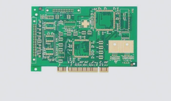
Common Errors in PCB Circuit Boards
(1) It is reported that NODE is not found when loading the network. The components used in the PCB library have inconsistent pin numbers with those in the schematic. For example, a transistor might have pin numbers e, b, and c in the schematic, but 1, 2, and 3 in the PCB.
(2) It is often impossible to print onto one page.
a. The issue may stem from not starting at the origin when creating the PCB library.
b. The component might have been moved and rotated multiple times, leaving hidden characters outside the PCB boundary. To address this, reveal all hidden characters, reduce the PCB size, and reposition the characters within the boundary.
(3) The DRC reporting network is divided into several parts:
This indicates that the network is not fully connected. Review the report file and use CONNECTED COPPER to locate the issue. For more complex designs, avoid relying solely on automatic routing.
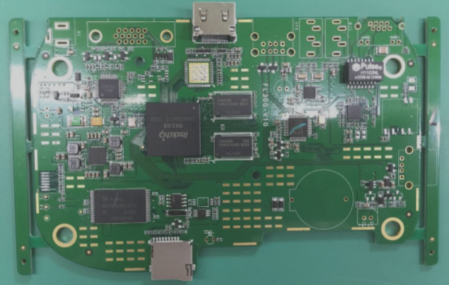
Common Mistakes in the Manufacturing Process of PCB Circuit Boards
(1) Pad Overlap:
a. Causes excessive drilling in one area, leading to broken drills and damaged holes.
b. In multi-layer boards, overlapping connection and isolation layers can cause errors related to isolation and connection.
(2) Irregular Use of Graphics Layers:
a. Design violations, such as placing component surfaces on the Bottom layer and soldering surfaces on the Top layer, can lead to confusion.
b. Excess design debris on each layer, such as broken lines, unnecessary borders, and labels, should be cleaned up.

(3) Unreasonable Characters
a. The characters cover SMD soldering tabs, causing inconvenience for PCB on-off detection and component soldering.
b. The characters are too small, making screen printing difficult. Conversely, if the characters are too large, they will overlap and become difficult to distinguish. The font size should generally be >40mil.
(4) Single-Sided Pad Setting Aperture
a. Single-sided pads are generally not drilled, so their aperture should be designed as zero. Otherwise, drilling data will show a hole at this position. Special instructions should be given if drilling is required.
b. If a single-sided pad needs to be drilled but the aperture is not designed, the software will treat this pad as an SMT pad when generating electrical and ground data, resulting in the loss of the isolation disk on the inner layer.
(5) Drawing PCB Pads with Filler Blocks
Although it may pass DRC inspection, solder mask data cannot be directly generated during processing. Consequently, the pad will be covered with solder mask and cannot be soldered.
(6) Electrical Ground Layer with Heat Sink and Signal Line
The positive and negative images are designed together, which may cause errors. Ensure that the heat sink and signal line are correctly separated.
(7) Large Area Grid Spacing Too Small
Grid line spacing less than 0.3mm can cause film breakage during the PCB manufacturing process, increasing processing difficulty.
(8) Graphics Too Close to the Frame
Ensure a minimum spacing of 0.2mm (V-cut >0.35mm). If the spacing is insufficient, copper foil may warp and solder resist may peel off during exterior processing, affecting appearance quality, including the inner copper layers of multilayer boards.
(9) Unclear Outline Frame Design
Many layers are designed with frames that do not overlap, making it difficult for PCB manufacturers to determine which lines to use. The standard frame should be designed on the mechanical layer or the BOARD layer, with clear internal hollowed-out parts.
(10) Uneven Graphic Design
Uneven pattern electroplating can lead to inconsistent coating thickness and even warping. Ensure even current distribution during plating.
(11) Short-Shaped Hole
The length-to-width ratio of a special-shaped hole should be >2:1, with a width >1.0mm. Otherwise, CNC drilling machines may not be able to process it.
(12) Milling Profile Positioning Holes Not Designed
If possible, design at least two positioning holes with a diameter >1.5mm in the PCB board.
(13) Aperture Not Clearly Marked
a. Aperture markings should use the metric system where possible, in increments of 0.05.
b. Combine apertures that can be grouped into a reservoir area.
c. Clearly mark the tolerances for metallized holes and special holes (such as crimp holes).
(14) Unreasonable Wiring in Inner Layer of Multilayer Board
a. Placing heat dissipation pads on isolation tape may lead to connection failures after drilling.
b. Gaps in the isolation belt design can lead to misunderstandings.
c. If the isolation band design is too narrow, it may be challenging to accurately judge the network.
(1) It is reported that NODE is not found when loading the network. The components used in the PCB library have inconsistent pin numbers with those in the schematic. For example, a transistor might have pin numbers e, b, and c in the schematic, but 1, 2, and 3 in the PCB.
(2) It is often impossible to print onto one page.
a. The issue may stem from not starting at the origin when creating the PCB library.
b. The component might have been moved and rotated multiple times, leaving hidden characters outside the PCB boundary. To address this, reveal all hidden characters, reduce the PCB size, and reposition the characters within the boundary.
(3) The DRC reporting network is divided into several parts:
This indicates that the network is not fully connected. Review the report file and use CONNECTED COPPER to locate the issue. For more complex designs, avoid relying solely on automatic routing.
Common Mistakes in the Manufacturing Process of PCB Circuit Boards
(1) Pad Overlap:
a. Causes excessive drilling in one area, leading to broken drills and damaged holes.
b. In multi-layer boards, overlapping connection and isolation layers can cause errors related to isolation and connection.
(2) Irregular Use of Graphics Layers:
a. Design violations, such as placing component surfaces on the Bottom layer and soldering surfaces on the Top layer, can lead to confusion.
b. Excess design debris on each layer, such as broken lines, unnecessary borders, and labels, should be cleaned up.
(3) Unreasonable Characters
a. The characters cover SMD soldering tabs, causing inconvenience for PCB on-off detection and component soldering.
b. The characters are too small, making screen printing difficult. Conversely, if the characters are too large, they will overlap and become difficult to distinguish. The font size should generally be >40mil.
(4) Single-Sided Pad Setting Aperture
a. Single-sided pads are generally not drilled, so their aperture should be designed as zero. Otherwise, drilling data will show a hole at this position. Special instructions should be given if drilling is required.
b. If a single-sided pad needs to be drilled but the aperture is not designed, the software will treat this pad as an SMT pad when generating electrical and ground data, resulting in the loss of the isolation disk on the inner layer.
(5) Drawing PCB Pads with Filler Blocks
Although it may pass DRC inspection, solder mask data cannot be directly generated during processing. Consequently, the pad will be covered with solder mask and cannot be soldered.
(6) Electrical Ground Layer with Heat Sink and Signal Line
The positive and negative images are designed together, which may cause errors. Ensure that the heat sink and signal line are correctly separated.
(7) Large Area Grid Spacing Too Small
Grid line spacing less than 0.3mm can cause film breakage during the PCB manufacturing process, increasing processing difficulty.
(8) Graphics Too Close to the Frame
Ensure a minimum spacing of 0.2mm (V-cut >0.35mm). If the spacing is insufficient, copper foil may warp and solder resist may peel off during exterior processing, affecting appearance quality, including the inner copper layers of multilayer boards.
(9) Unclear Outline Frame Design
Many layers are designed with frames that do not overlap, making it difficult for PCB manufacturers to determine which lines to use. The standard frame should be designed on the mechanical layer or the BOARD layer, with clear internal hollowed-out parts.
(10) Uneven Graphic Design
Uneven pattern electroplating can lead to inconsistent coating thickness and even warping. Ensure even current distribution during plating.
(11) Short-Shaped Hole
The length-to-width ratio of a special-shaped hole should be >2:1, with a width >1.0mm. Otherwise, CNC drilling machines may not be able to process it.
(12) Milling Profile Positioning Holes Not Designed
If possible, design at least two positioning holes with a diameter >1.5mm in the PCB board.
(13) Aperture Not Clearly Marked
a. Aperture markings should use the metric system where possible, in increments of 0.05.
b. Combine apertures that can be grouped into a reservoir area.
c. Clearly mark the tolerances for metallized holes and special holes (such as crimp holes).
(14) Unreasonable Wiring in Inner Layer of Multilayer Board
a. Placing heat dissipation pads on isolation tape may lead to connection failures after drilling.
b. Gaps in the isolation belt design can lead to misunderstandings.
c. If the isolation band design is too narrow, it may be challenging to accurately judge the network.