File Types for PCB Design Input and Output
Introduction to PCB Design
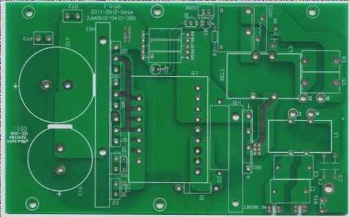
A Printed Circuit Board (PCB), also known as a printed circuit board, is an essential electronic component that provides support for electronic parts and facilitates electrical connections between them. PCBs have been a fundamental part of the electronics industry since the early days of connecting carbon and silicon chips to create functional electronic devices. The evolution of the design process has made PCB design more accessible and efficient for engineers.
Key Aspects of PCB Design
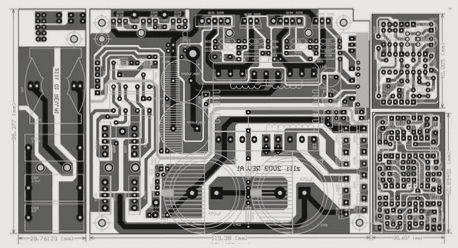
The PCB design process involves stages such as schematic design, PCB layout, circuit simulation, CAM engineering software, and board copy software. PCB design software typically includes schematic design and PCB layout modules, with some advanced tools integrating additional features.
File Types for PCB Design Input and Output
During the post-processing phase of PCB design, various file formats are used for input and output. Understanding these key file types is crucial in the industry.

PCB Design Input Data
- Schematic Diagram: The schematic diagram illustrates the circuit design principles and component relationships, serving as the foundation for PCB design.
- Structural Element Diagram: Defines the PCB’s size, shape, and component placement requirements.
- Design Requirements: Includes engineering requirement forms and reference documents.
- Engineering Requirements Form Content: Specifies layout and routing specifications for signal traces, board thickness, impedance, spacing, and power supply requirements.
Output Data After PCB Design Completion
- Assembly Documents: Include assembly files with naming conventions for easy identification.
- Gerber Files: Essential files for manufacturing processes.
- Stencil Files: Used for solder paste application during assembly.
- Structural Documents: Provide structural information for the PCB.
- PCB Source Files: Final output files compiled for testing, processing, and assembly.
Ensuring the proper handling of these input and output files is essential for successful PCB design and production processes.


