PCBA Process Overview
PCBA, or Printed Circuit Board Assembly, is a comprehensive process that involves various stages to ensure the production of high-quality electronic products. At Gaotuo, we adhere to stringent quality control measures throughout the following key stages:
1. PCB Circuit Board Manufacturing
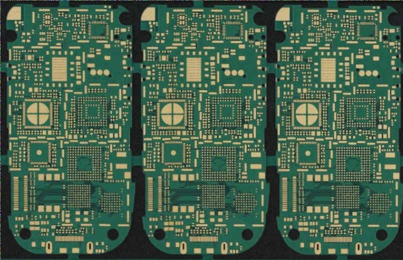
When we receive a PCBA order, our first step is to analyze the Gerber file meticulously. We pay close attention to factors such as PCB hole spacing, load-bearing capacity, and considerations for high-frequency signal interference and impedance during wiring design to prevent bending or breakage.
2. Component Procurement and Inspection
Component procurement is a critical phase that requires strict channel control to source materials exclusively from reputable traders and original manufacturers. Our dedicated inspection station conducts rigorous checks on incoming components to ensure their quality and authenticity. Some key inspection aspects include:
- PCB: Temperature tests, checking for flying leads, blocked vias, ink leakage, and verifying board surface flatness.
- IC: Verification of silk screen accuracy and maintaining stable temperature and humidity levels.
- Other materials: Inspection of silk screen, appearance, and power-on measurements through random sampling.
3. SMT Chip Processing
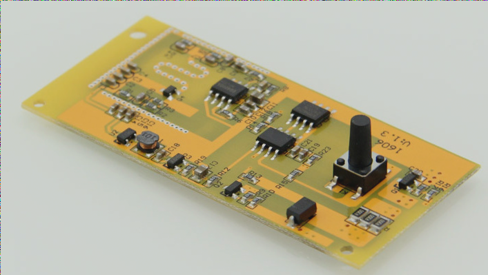
Control over solder paste printing and reflow oven temperatures is crucial during SMT patch processing. Utilizing high-quality laser stencils and adhering to strict reflow soldering guidelines are essential for reliable soldering. AOI testing is implemented to minimize defects.
4. Plug-in Processing
DIP plug-in processing emphasizes mold design optimization for wave soldering to enhance post-furnace product success rates. Continuous refinement of mold design by PE engineers is key.
5. Program Flashing
Customers are advised to include test points on the PCB during the DFM report for testing circuit continuity post-component soldering. Providing a program for the main control IC enables thorough evaluation of functional changes and overall PCBA functionality.
6. Testing and Aging
PCBA board testing involves key assessments such as ICT, FCT, aging tests, temperature and humidity evaluations, and drop tests. These tests are conducted according to the customer’s test plan with detailed reporting data.


