Printed Circuit Boards: Design Principles and Anti-Interference Measures
Introduction
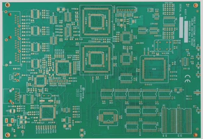
Printed circuit boards (PCBs) are essential components in electronic products, facilitating electrical connections between various elements and systems. With advancing power technology, PCB density is increasing rapidly, underscoring the importance of adhering to design principles and anti-interference measures.
General Principles of PCB Design
Optimizing electronic circuit performance requires careful consideration of component placement and wiring layout. When designing a PCB for a balance of quality and cost-effectiveness, the following principles should guide the process:
Layout
- Size Consideration: PCB size impacts trace length, impedance, noise immunity, and costs. It’s crucial to find a size that balances these factors.
- Component Placement: Special components should be strategically placed based on the circuit’s functional units.
- Special Component Placement Principles:
- Minimize connection lengths for high-frequency components to reduce parasitic parameters and interference.
- Avoid placing interference-sensitive components close together; keep input and output components apart.
- Increase spacing for components with high potential differences to prevent short circuits.
- Secure heavy components (>15g) with brackets before soldering.
- Position heating elements away from other heat-generating components.
- Strategically place adjustable components for easy access and alignment with external adjustments.
- Allocate space for positioning holes and fixing brackets according to circuit unit arrangement.
- Circuit Component Arrangement Principles:
- Position functional circuit units based on signal flow for optimal signal transmission.
- Center core components with surrounding elements arranged neatly and compactly.
- Minimize trace lengths and connections between components.
- Consider parasitic parameters in high-frequency circuits and use parallel connections where possible.
- Keep components at least 2mm away from PCB edges; prefer a rectangular board shape with specific aspect ratios for larger boards.
Wiring
- Avoid running input and output wires parallel; use ground wires between signal lines to prevent feedback coupling.
- Choose trace widths based on bond strength and current requirements to prevent excessive temperature rises.
Latest Insights
Recent advancements in PCB design include the integration of AI algorithms to optimize component placement for enhanced signal flow and reduced interference. Additionally, the use of advanced materials with improved thermal conductivity has led to more efficient heat dissipation in PCBs, improving overall system reliability.
PCB Design Best Practices
-
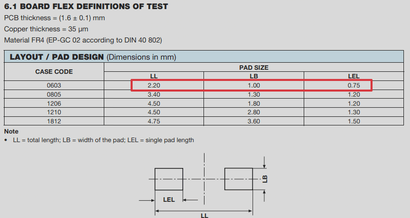
Trace Width and Spacing
For integrated circuits and digital circuits, trace widths typically range from 0.02mm to 0.3mm. Wider traces, especially for power and ground lines, are recommended to improve performance.
The spacing between wires should be determined by insulation resistance and breakdown voltage, with a minimum spacing of 5~8mm for digital circuits.
Printed traces at corners should be arc-shaped to avoid performance degradation in high-frequency circuits.
-
Soldering Pad Hole Sizes
The center hole of a soldering pad should be slightly larger than the lead diameter to avoid cold joints.
For high-density digital circuits, the ideal minimum pad diameter is (d + 1.0)mm.
-
Anti-Interference Measures
Power Line Design
Power lines should be wide to reduce loop resistance and aligned with ground and signal lines for improved noise immunity.
Ground Wire Design
Separate digital and analog grounds, use thick ground traces, and employ a closed-loop ground configuration for noise resistance.
Decoupling Capacitor Configuration
Place decoupling capacitors strategically, following guidelines for different components to reduce noise and power fluctuations.