1.1 **PCB Proofing Definition**
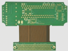
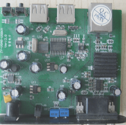
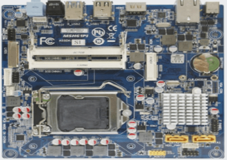
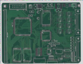
PCB proofing refers to the trial production of printed circuit boards (PCBs) before full-scale manufacturing. It primarily involves the process where electronic engineers design the circuit, finalize the PCB layout, and then send it for small-batch production at the factory, which is known as PCB proofing. Typically, engineers conduct PCB proofing before the product design is finalized and thoroughly tested. In simple terms, proofing means creating samples; PCB proofing specifically refers to fabricating a physical version of the designed PCB schematic, serving as a product test before mass production begins. A PCB project involves several critical steps, and any issue in one stage can significantly impact the overall product development timeline. This is also true for PCB manufacturing. Typically, the PCB design will be sent to a prototype factory for proofing, where a limited number of boards are produced. Testing is then conducted, and if successful, mass production can proceed. The cost of mass production will be significantly lower than the prototype stage, with the primary focus of proofing being speed.
1.2 **PCB Proofing Files**
PCB proofing files usually consist of PCB files or Gerber files, along with instructions for board fabrication. These instructions detail aspects such as the number of layers, materials, pad design, ink color, and whether impedance matching is required.
**1.3 PCB Proofing Cycle**
The typical PCB proofing cycle is around 7 days, although it can be expedited if needed.
– Single and double-sided boards are typically delivered within 7 days.
– Four-layer boards usually take about 15 days for proofing.
– Mass production generally takes around 20 to 30 days, depending on the production capacity of the specific factory.
**2. PCB Proofing Instructions**
PCB proofing generally involves several key details, including the PCB’s chip size, joint size, material type, quantity, thickness, copper thickness, surface treatment, solder mask color, text color, environmental protection requirements, fire rating, via plug specifications, hole tolerances, warpage, molding methods, etc. Below are some key items to note:
**2.1 Material**:
It’s important to specify the type of material used for the PCB. The most common material is FR4, but special materials include Rogers, Taconic, PTFE (Teflon), and F4B (high-frequency board).
**2.2 Layers**:
Indicate the number of layers required for the PCB.
**2.3 Solder Mask Color**:
The solder mask color should be specified according to the company’s requirements, with green being the most common choice.
**2.4 Silkscreen Color**:
Typically, the color of the silkscreen (text and borders) on the PCB is white.
**2.5 Copper Thickness**:
The copper thickness is generally calculated based on the current requirements of the PCB circuit. While thicker copper is often better, it increases the cost, so a balance must be struck to ensure both performance and cost-effectiveness.
**2.6 Via Solder Mask Coverage**:
Specify whether the vias should be covered by solder mask. If they are covered, it insulates the vias; otherwise, they remain uninsulated.
**2.7 Surface Coating**:
The surface coating options include spray tin, OSP (Organic Solderability Preservative), tin-lead, gold sinking, and gold plating, among others.
**2.8 Quantity**:
Clearly state the quantity of PCBs to be produced.
**3. Precautions for PCB Proofing**
**3.2.1**
Carefully review all PCB documentation to avoid data errors.
**3.2.2**
Ensure that all process approvals and configurations are finalized with the PCB manufacturer.
**3.2.3**
Control the production quantity to save costs while ensuring quality.
**4.2.4**
Maintain clear communication with the manufacturer to proactively avoid any potential issues.
**4. PCB Proofing Method Selection**
There are three common methods for PCB proofing: regular PCB factories, specialized prototype companies, and some PCB copyboard companies.
**4.1**
The goal of using a regular PCB factory for proofing is usually to place large volume orders. These factories aim for repeat business. In contrast, professional proofing companies specialize in making samples or small batches, offering fast and professional service. They are suitable for one or two small sample runs but cannot handle large orders.
**4.2**
In terms of quality assurance, regular PCB factories typically provide better results than prototype companies. A professional prototype company may not perform flying probe tests, and any quality issues will require another batch to be ordered. Regular PCB factories, however, usually conduct flying probe tests, ensuring more rigorous quality control from materials through to the process, which often results in successful outcomes on the first attempt.
**4.3**
Some small PCB copy companies also engage in proofing. After receiving the materials and finalizing the plan, these companies quickly produce and test functional prototypes to ensure feasibility.
**5. PCB Proofing Market Distribution**
The demand for PCB proofing is primarily concentrated in regions with a high level of electronic product development.
If you have any PCB manufacturing needs, please do not hesitate to contact me.Contact me

