The anti-interference issue is a critical aspect of modern PCB circuit design, as it directly impacts the performance and reliability of the entire system. Currently, the main anti-jamming technologies employed in systems are hardware-based and software-based solutions.
1) **Hardware anti-jamming technology design**: The carrier signal of the inverter circuit in the flywheel energy storage system, which can reach frequencies up to 20 kHz, inherently generates noise. This results in noise and harmonic disturbances caused by the power electronic devices within the system, which become the primary sources of interference. The extent of this interference on the equipment and surrounding instruments depends on factors such as the anti-jamming capability of the control system and devices, the wiring environment, the installation distance, and the grounding methods employed.
2) **Software anti-jamming technology**:

In addition to implementing a range of anti-jamming measures at the hardware level, software measures such as digital filtering, setting software traps, and employing watchdog redundancy design should be used to ensure stable and reliable system operation. Particularly when the energy storage flywheel operates in a specific state for an extended period, continuous monitoring of this state within the main loop is necessary, with corresponding actions taken as needed. This approach also serves to enhance system reliability.
The anti-interference design of the printed circuit board (PCB) is closely tied to the specifics of the PCB layout. Below is a collection of comprehensive and detailed principles for PCB anti-interference design.
The specific principles are as follows:
1. **Component Layout**
1. Avoid excessively long parallel signal traces.
2. Ensure the clock input terminals of the PCB clock generator, crystal oscillator, and CPU are as close as possible while keeping them away from other low-frequency components.
3. Components should be arranged around core components, and trace lengths should be kept as short as possible.
4. Implement a partitioned layout for the PCB.
5. Take into account the position and orientation of the PCB within the chassis.
6. Minimize trace lengths between high-frequency components.
2. **Decoupling Capacitor Configuration**
1. Include a 10µF capacitor for every 10 integrated circuits.
2. Use leaded capacitors for low-frequency decoupling, and chip capacitors for high-frequency decoupling.
3. Place a 0.1µF ceramic capacitor near each integrated circuit.
4. For devices that experience significant power changes during shutdown, use high-frequency decoupling capacitors to improve noise immunity.
5. Avoid sharing vias between capacitors.
6. Keep the leads of decoupling capacitors as short as possible.
3. **Power Trace Design**
1. Select an appropriate power supply.
2. Make power traces as wide as possible.
3. Ensure that the power trace direction aligns with the bottom trace and data transmission directions.
4. Incorporate anti-interference components where necessary.
5. Place a decoupling capacitor (10-100µF) at the power inlet.
4. **Grounding Design**
1. Separate analog and digital grounds.
2. Aim for a single-point grounding system where feasible.
3. Widen ground traces as much as possible.
4. Connect sensitive circuits to a stable ground reference point.
5. Design the PCB layout to isolate high-bandwidth noise circuits from low-frequency circuits.
6. Minimize the area of ground loops (the path formed by all components returning to ground after being grounded).
If you have any PCB manufacturing needs, please do not hesitate to contact me.Contact me
1) **Hardware anti-jamming technology design**: The carrier signal of the inverter circuit in the flywheel energy storage system, which can reach frequencies up to 20 kHz, inherently generates noise. This results in noise and harmonic disturbances caused by the power electronic devices within the system, which become the primary sources of interference. The extent of this interference on the equipment and surrounding instruments depends on factors such as the anti-jamming capability of the control system and devices, the wiring environment, the installation distance, and the grounding methods employed.
2) **Software anti-jamming technology**:
In addition to implementing a range of anti-jamming measures at the hardware level, software measures such as digital filtering, setting software traps, and employing watchdog redundancy design should be used to ensure stable and reliable system operation. Particularly when the energy storage flywheel operates in a specific state for an extended period, continuous monitoring of this state within the main loop is necessary, with corresponding actions taken as needed. This approach also serves to enhance system reliability.
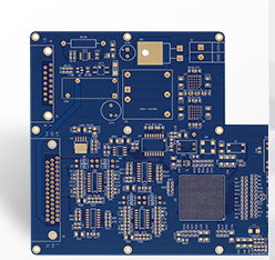
The anti-interference design of the printed circuit board (PCB) is closely tied to the specifics of the PCB layout. Below is a collection of comprehensive and detailed principles for PCB anti-interference design.
The specific principles are as follows:
1. **Component Layout**
1. Avoid excessively long parallel signal traces.
2. Ensure the clock input terminals of the PCB clock generator, crystal oscillator, and CPU are as close as possible while keeping them away from other low-frequency components.
3. Components should be arranged around core components, and trace lengths should be kept as short as possible.
4. Implement a partitioned layout for the PCB.
5. Take into account the position and orientation of the PCB within the chassis.
6. Minimize trace lengths between high-frequency components.
2. **Decoupling Capacitor Configuration**
1. Include a 10µF capacitor for every 10 integrated circuits.
2. Use leaded capacitors for low-frequency decoupling, and chip capacitors for high-frequency decoupling.
3. Place a 0.1µF ceramic capacitor near each integrated circuit.
4. For devices that experience significant power changes during shutdown, use high-frequency decoupling capacitors to improve noise immunity.
5. Avoid sharing vias between capacitors.
6. Keep the leads of decoupling capacitors as short as possible.
3. **Power Trace Design**
1. Select an appropriate power supply.
2. Make power traces as wide as possible.
3. Ensure that the power trace direction aligns with the bottom trace and data transmission directions.
4. Incorporate anti-interference components where necessary.
5. Place a decoupling capacitor (10-100µF) at the power inlet.
4. **Grounding Design**
1. Separate analog and digital grounds.
2. Aim for a single-point grounding system where feasible.
3. Widen ground traces as much as possible.
4. Connect sensitive circuits to a stable ground reference point.
5. Design the PCB layout to isolate high-bandwidth noise circuits from low-frequency circuits.
6. Minimize the area of ground loops (the path formed by all components returning to ground after being grounded).
If you have any PCB manufacturing needs, please do not hesitate to contact me.Contact me

