PCB Design Best Practices
When designing a PCB, it is crucial to adhere to specific requirements and follow established guidelines to ensure optimal performance. Here are some basic principles to consider:
1. Collaboration and Specification
- Engage with relevant personnel to meet requirements for structure, signal integrity, manufacturing, testability, and electromagnetic compatibility.
2. Component Placement
- Position critical components like connectors and indicator lights based on structural diagrams.
3. Prohibited Areas
- Designate areas where wiring and layout are restricted based on device requirements.
4. Process Flow Selection
- Consider PCB performance and manufacturing efficiency when choosing the process flow.
5. Layout Optimization
- Minimize wiring length, separate signal types, and ensure proper spacing for components.
6. Modular Layout
- Implement a symmetrical modular layout for identical circuit sections.
7. Grid Settings
- Use recommended grid sizes for layout settings to ensure proper spacing.
8. Wiring Considerations
- Choose wire width and spacing wisely based on process conditions and density requirements.
9. Line Orientation
- Orient adjacent wiring layers to minimize parasitic capacitance.
10. Signal Integrity
- Keep printed trace wiring short for high-frequency signals and sensitive lines.
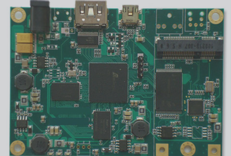
For a detailed guide on PCB design principles and best practices, refer to the image below:

Trace Width and Spacing Recommendations
1. Line Width/Spacing
- Recommended line width/spacing is ≥5mil/5mil, with a minimum usable width/spacing of 4mil/4mil.
2. Distance Guidelines
- Maintain appropriate distances between traces, pads, and solder mask openings to prevent interference.
Safety Distance and Routing
1. Edge Clearance
- Ensure a safety distance of >20mil between traces and the board edge to prevent short circuits.
2. Grounding Considerations
- Maintain proper separation between grounding elements and the board edge to avoid interference.
3. Restricted Wiring Zones
- Avoid routing in areas where metal components directly contact the PCB to prevent potential issues.
Key Considerations for PCB Layout Optimization
Shortest Distance Between Trace and Non-Metallized Hole
When designing a PCB layout, it is crucial to maintain the shortest distance between traces and non-metallized holes to prevent signal interference and ensure signal integrity.
Essential Principles of Multi-Layer PCB Layout
- The bottom layer, acting as the ground plane, shields the device and serves as a reference for surface wiring.
- Position signal layers close to the ground plane to minimize interference.
- Avoid placing adjacent signal layers to prevent crosstalk.
- Proximity of the main power supply is vital for efficient operation.
- Adopt a symmetrical design for uniformity in dielectric and copper foil thickness.
Best Practices for Silk Screen Design
- Ensure legibility by using a silk screen line width exceeding 5 mils and a height of at least 50 mils.
- Avoid overlapping silk screen with pads or reference points.
- Default silk screen ink color is white; specify any special requirements in the drilling file.
- Customize silk screen content in high-density PCBs based on specific needs.
- Arrange silk-screened strings from left to right and bottom to top for clarity.
If you require PCB manufacturing services, feel free to contact us.


