PCB board cutting is a crucial step in PCB design. However, many designers hesitate to engage in this task due to the involvement of sandpaper grinding (a hazardous task) and the repetitive nature of line drawing (a simple, monotonous job). In fact, many designers believe that PCB cutting is not a technical task and that even junior designers can handle it with minimal training. While this view has some merit, like many tasks, PCB board cutting requires specific skills. When designers master these skills, they can save significant time and reduce labor intensity. Below, we will explore this knowledge in more detail.
1. **The Concept of PCB Board Cutting**
PCB board cutting refers to the process of extracting the schematic diagram and board layout (PCB layout) from the original PCB. The goal is to prepare the board for subsequent development activities, such as component installation, in-depth testing, circuit modifications, and more. While these activities are closely related to PCB cutting, they fall outside its direct scope and will not be covered in detail here.
2. **The Process of PCB Board Cutting**

1. Remove the components from the original board.
2. Scan the original board to generate the graphic file.
3. Grind off the surface layer to expose the intermediate layer.
4. Scan the intermediate layer to create the graphic file.
5. Repeat steps 2-4 until all layers are processed.
6. Use specialized software to convert the graphic files into electrical relationship files—PCB diagrams. With the right software, the designer only needs to trace the graphics once.
7. Verify and finalize the design.
**Third, Skills for PCB Board Cutting**
Cutting a PCB, especially a multi-layer PCB, is a labor-intensive and time-consuming task that involves much repetitive work. Designers must be patient and meticulous, as mistakes can easily occur. The key to successful PCB cutting is to use the right software to automate repetitive tasks, saving time and ensuring accuracy.
1. **A scanner is essential during the cutting process.**
Many designers habitually draw directly on PCB design systems like PROTEL, PADSOR, or CAD, which is not ideal. The scanned graphic file serves not only as the basis for converting to a PCB file but also as a reference for later inspection. Using a scanner significantly reduces manual labor and effort. It’s not an exaggeration to say that, with proper use of a scanner, even individuals without design experience can perform PCB board cutting tasks effectively.
2. **Grind the board in one direction.**
In an effort to speed up the process, some designers opt for two-way grinding (i.e., grinding from both the front and rear surfaces toward the middle layer). This approach is problematic, as it can easily cause the board to be over-ground, potentially damaging other layers. The outer layer of the PCB is the hardest due to the craftsmanship, copper foil, and pads, while the middle layer is the softest. This makes grinding through the intermediate layers especially difficult and risky. Moreover, since materials, hardness, and elasticity can vary between manufacturers, accurate grinding can be challenging.
3. **Select high-quality conversion software.**
Converting scanned graphic files into PCB files is the most critical step of the entire process. With good conversion software, the designer only needs to trace the graphics once, simplifying the work considerably. EDA2000 is highly recommended here, as it offers great convenience and ease of use.
1. **The Concept of PCB Board Cutting**
PCB board cutting refers to the process of extracting the schematic diagram and board layout (PCB layout) from the original PCB. The goal is to prepare the board for subsequent development activities, such as component installation, in-depth testing, circuit modifications, and more. While these activities are closely related to PCB cutting, they fall outside its direct scope and will not be covered in detail here.
2. **The Process of PCB Board Cutting**
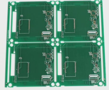
1. Remove the components from the original board.
2. Scan the original board to generate the graphic file.
3. Grind off the surface layer to expose the intermediate layer.
4. Scan the intermediate layer to create the graphic file.
5. Repeat steps 2-4 until all layers are processed.
6. Use specialized software to convert the graphic files into electrical relationship files—PCB diagrams. With the right software, the designer only needs to trace the graphics once.
7. Verify and finalize the design.
**Third, Skills for PCB Board Cutting**
Cutting a PCB, especially a multi-layer PCB, is a labor-intensive and time-consuming task that involves much repetitive work. Designers must be patient and meticulous, as mistakes can easily occur. The key to successful PCB cutting is to use the right software to automate repetitive tasks, saving time and ensuring accuracy.
1. **A scanner is essential during the cutting process.**
Many designers habitually draw directly on PCB design systems like PROTEL, PADSOR, or CAD, which is not ideal. The scanned graphic file serves not only as the basis for converting to a PCB file but also as a reference for later inspection. Using a scanner significantly reduces manual labor and effort. It’s not an exaggeration to say that, with proper use of a scanner, even individuals without design experience can perform PCB board cutting tasks effectively.
2. **Grind the board in one direction.**
In an effort to speed up the process, some designers opt for two-way grinding (i.e., grinding from both the front and rear surfaces toward the middle layer). This approach is problematic, as it can easily cause the board to be over-ground, potentially damaging other layers. The outer layer of the PCB is the hardest due to the craftsmanship, copper foil, and pads, while the middle layer is the softest. This makes grinding through the intermediate layers especially difficult and risky. Moreover, since materials, hardness, and elasticity can vary between manufacturers, accurate grinding can be challenging.
3. **Select high-quality conversion software.**
Converting scanned graphic files into PCB files is the most critical step of the entire process. With good conversion software, the designer only needs to trace the graphics once, simplifying the work considerably. EDA2000 is highly recommended here, as it offers great convenience and ease of use.

