
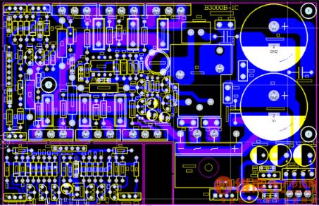
Understanding the Elements of PCB Design
- Pad: A metalized hole for soldering component pins.
- Via: A hole facilitating connections between different layers.
- Mounting Hole: Secures the PCB in place.
- Trace: Copper pathway connecting component pins.
- Connector: Establishes electrical connections between circuit boards.
- Fill: Copper plating for grounding networks, reducing impedance.
- Electrical Boundary: Defines the physical edge of the PCB.
Types of PCB Layer Configurations
Printed circuit boards come in various layer configurations, including:
- Single-layer board: Copper on one side, primarily for routing and soldering.
- Double-layer board: Copper on both sides, used for component placement and soldering.
- Multilayer board: Consists of multiple functional layers for routing, signal transmission, and more.
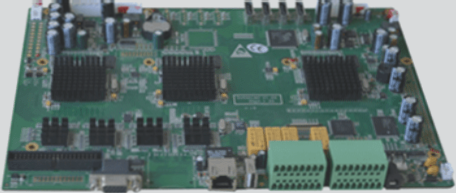
Functional Layers of a Printed Circuit Board
The PCB includes various functional layers:
- Signal Layer: For component placement and trace routing.
- Protective Layer: Ensures areas not requiring tinning remain untinned.
- Silkscreen Layer: Prints component information and logos.
- Internal Layer: Used for signal routing.
- Other Layers: Drill Guide, Keep-Out, Drill Drawing, and Multi-Layer layers.
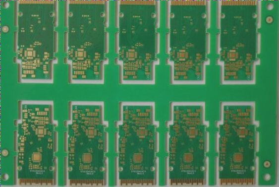
Component Packaging in PCB Layout Design
Component packaging in PCB layout design is crucial for determining the external appearance and positioning of solder joints when mounting components. It plays a vital role in placing, securing, and protecting the chip, while also serving as a bridge between the chip’s internal circuitry and the outside world.
It is important to understand that different components can share the same package, and a single component may be available in various package types. Therefore, when designing a PCB, it is essential to not only know the component’s name and model but also its specific package type.
Common package types in PCB design include through-hole (in-line) and surface-mount packages. In through-hole packaging, the component’s pins are inserted through vias and soldered on the opposite side of the board. On the other hand, surface-mount packaging involves directly placing the component onto pads on the board’s surface, with connections established solely through these surface pads.

 العربية
 简体中文
简体中文 Nederlands
 English
 Français
 Deutsch
 Italiano
 日本語
日本語 한국어
한국어 Português
 Русский
 Español
 ไทย
ไทย