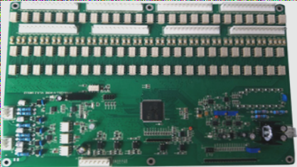
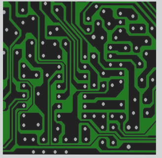
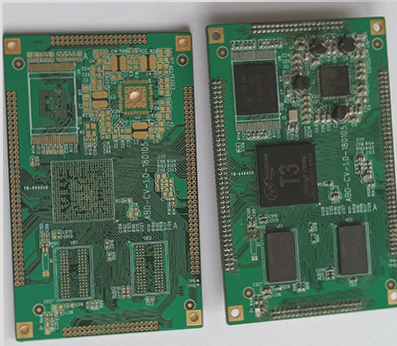
1. One challenge in contemporary mixed-signal PCB design is the increasing variety of digital logic devices, including GTL, LVTTL, LVCMOS, and LVDS logic. Each type has distinct logic thresholds and voltage swings, yet these differing parameters must be integrated into a single PCB design. Through comprehensive analysis of high-density, high-performance mixed-signal PCB layouts and wiring strategies, one can master effective techniques and approaches.
Analysis of Layout and Wiring Methods for Mixed-Signal PCB Design
Fundamentals of Mixed-Signal Circuit Wiring
When digital and analog circuits share components on the same board, the layout and wiring must be approached systematically.
2. In mixed-signal PCB design, there are specific requirements for power supply routing, necessitating the isolation of analog noise from digital circuit noise to prevent coupling. This requirement adds to the complexity of layout and wiring. The stringent criteria for power transmission lines, along with the need to keep noise coupling between analog and digital circuits separate, significantly enhance the complexity of mixed-signal PCB design.
3. If the power supply for the analog amplifier in the A/D converter is combined with the digital power supply, it can lead to interference between the analog and digital sections of the circuit. Additionally, due to the positioning of input/output connectors, the layout may require a mix of digital and analog wiring.
Before proceeding with layout and routing, engineers must identify the fundamental weaknesses in the proposed layout and routing strategies. Even with misjudgments, many engineers rely on layout and wiring data to uncover potential electrical issues.

4. Layout and Wiring of Modern Mixed-Signal PCBs
This section will illustrate the techniques involved in mixed-signal PCB layout and routing through the design of the OC48 interface card. OC48, which stands for Optical Carrier Standard 48, is primarily aimed at 2.5Gb serial optical communication. It represents one of the high-capacity optical communication standards in contemporary equipment. The OC48 interface card encompasses several typical challenges associated with mixed-signal PCB layout and wiring. The layout and wiring process will detail the sequence and steps necessary for an effective mixed-signal PCB layout scheme.
The OC48 card features an optical transceiver that facilitates the bidirectional conversion of optical signals and analog electrical signals. Analog signals are input to or output from a digital signal processor (DSP), which converts these analog signals into digital logic levels. This allows for connections to various components such as microprocessors, programmable gate arrays, and the DSP interface circuit on the OC48 card. The design also integrates an independent phase-locked loop, power filter, and local reference voltage source.
5. Upon reviewing the layout and wiring requirements of various functional circuit blocks, a 12-layer board is initially suggested. The arrangement of microstrip and stripline layers can effectively minimize the coupling between adjacent wiring layers while enhancing impedance control. A grounding layer is positioned between the first and second layers to isolate the wiring for sensitive analog reference sources, CPU cores, and PLL filter power supplies from the microprocessor and DSP components on the first layer. Power and ground planes are always paired, consistent with the implementation on the OC48 card for the shared 3.3V power plane. This approach reduces the impedance between the power supply and ground, thereby diminishing noise on the power signal.
6. It is essential to avoid routing digital clock lines and high-frequency analog signal lines near the power layer, as this can result in noise coupling from the power signal to the sensitive analog signals. When designing digital signal wiring, it’s crucial to carefully consider the use of openings (splits) in the power and analog ground planes, particularly at the input and output terminals of mixed-signal devices. Routing through an opening in an adjacent signal layer may cause impedance discontinuities and poor transmission line loops, leading to signal quality, timing, and EMI issues.
Occasionally, incorporating additional ground layers or using multiple outer layers for the local power or ground layer beneath a device can eliminate the need for openings, thereby avoiding these complications. The OC48 interface card employs multiple ground layers. Maintaining the stacking symmetry of the opening layer and the wiring layers helps prevent card deformation and simplifies the manufacturing process. Since 1-ounce copper clad laminates exhibit high resistance to large currents, they should be used for the 3.3V power layer and its corresponding ground layer, while 0.5-ounce copper clad laminates can be utilized for other layers. This configuration helps mitigate transient high currents or spikes due to voltage fluctuations.
7. When designing a complex system from the ground plane up, it is advisable to use cards with thicknesses of 0.093 inches and 0.100 inches to support the wiring layer and ground isolation layer. The card thickness must also be adjusted based on the dimensions of the via pads and the wiring characteristics of the holes, ensuring that the aspect ratio of the hole diameter to the thickness of the finished card does not exceed the aspect ratio for metallized holes specified by the manufacturer.
For those aiming to design a cost-effective, high-yield commercial product with minimal wiring layers, careful consideration of the wiring details for all specialized power supplies on the mixed-signal PCB is essential before layout or routing. Prior to initiating the layout and routing process, it is beneficial to have the target manufacturer review the preliminary layering plan. The layering should fundamentally depend on the thickness of the finished product, the number of layers, copper weight, impedance (with tolerance), and the size of the smallest via pads and holes. The manufacturer should provide a documented layering recommendation.
This recommendation should encompass all configuration examples of controlled impedance stripline and microstrip lines. You need to integrate your impedance predictions with those from the manufacturer. Subsequently, use these impedance predictions to validate the signal routing characteristics in the simulation tool employed for developing CAD routing rules.
If you have any PCB manufacturing needs, please do not hesitate to contact me.Contact me
Analysis of Layout and Wiring Methods for Mixed-Signal PCB Design
Fundamentals of Mixed-Signal Circuit Wiring
When digital and analog circuits share components on the same board, the layout and wiring must be approached systematically.
2. In mixed-signal PCB design, there are specific requirements for power supply routing, necessitating the isolation of analog noise from digital circuit noise to prevent coupling. This requirement adds to the complexity of layout and wiring. The stringent criteria for power transmission lines, along with the need to keep noise coupling between analog and digital circuits separate, significantly enhance the complexity of mixed-signal PCB design.
3. If the power supply for the analog amplifier in the A/D converter is combined with the digital power supply, it can lead to interference between the analog and digital sections of the circuit. Additionally, due to the positioning of input/output connectors, the layout may require a mix of digital and analog wiring.
Before proceeding with layout and routing, engineers must identify the fundamental weaknesses in the proposed layout and routing strategies. Even with misjudgments, many engineers rely on layout and wiring data to uncover potential electrical issues.

4. Layout and Wiring of Modern Mixed-Signal PCBs
This section will illustrate the techniques involved in mixed-signal PCB layout and routing through the design of the OC48 interface card. OC48, which stands for Optical Carrier Standard 48, is primarily aimed at 2.5Gb serial optical communication. It represents one of the high-capacity optical communication standards in contemporary equipment. The OC48 interface card encompasses several typical challenges associated with mixed-signal PCB layout and wiring. The layout and wiring process will detail the sequence and steps necessary for an effective mixed-signal PCB layout scheme.
The OC48 card features an optical transceiver that facilitates the bidirectional conversion of optical signals and analog electrical signals. Analog signals are input to or output from a digital signal processor (DSP), which converts these analog signals into digital logic levels. This allows for connections to various components such as microprocessors, programmable gate arrays, and the DSP interface circuit on the OC48 card. The design also integrates an independent phase-locked loop, power filter, and local reference voltage source.
5. Upon reviewing the layout and wiring requirements of various functional circuit blocks, a 12-layer board is initially suggested. The arrangement of microstrip and stripline layers can effectively minimize the coupling between adjacent wiring layers while enhancing impedance control. A grounding layer is positioned between the first and second layers to isolate the wiring for sensitive analog reference sources, CPU cores, and PLL filter power supplies from the microprocessor and DSP components on the first layer. Power and ground planes are always paired, consistent with the implementation on the OC48 card for the shared 3.3V power plane. This approach reduces the impedance between the power supply and ground, thereby diminishing noise on the power signal.
6. It is essential to avoid routing digital clock lines and high-frequency analog signal lines near the power layer, as this can result in noise coupling from the power signal to the sensitive analog signals. When designing digital signal wiring, it’s crucial to carefully consider the use of openings (splits) in the power and analog ground planes, particularly at the input and output terminals of mixed-signal devices. Routing through an opening in an adjacent signal layer may cause impedance discontinuities and poor transmission line loops, leading to signal quality, timing, and EMI issues.
Occasionally, incorporating additional ground layers or using multiple outer layers for the local power or ground layer beneath a device can eliminate the need for openings, thereby avoiding these complications. The OC48 interface card employs multiple ground layers. Maintaining the stacking symmetry of the opening layer and the wiring layers helps prevent card deformation and simplifies the manufacturing process. Since 1-ounce copper clad laminates exhibit high resistance to large currents, they should be used for the 3.3V power layer and its corresponding ground layer, while 0.5-ounce copper clad laminates can be utilized for other layers. This configuration helps mitigate transient high currents or spikes due to voltage fluctuations.
7. When designing a complex system from the ground plane up, it is advisable to use cards with thicknesses of 0.093 inches and 0.100 inches to support the wiring layer and ground isolation layer. The card thickness must also be adjusted based on the dimensions of the via pads and the wiring characteristics of the holes, ensuring that the aspect ratio of the hole diameter to the thickness of the finished card does not exceed the aspect ratio for metallized holes specified by the manufacturer.
For those aiming to design a cost-effective, high-yield commercial product with minimal wiring layers, careful consideration of the wiring details for all specialized power supplies on the mixed-signal PCB is essential before layout or routing. Prior to initiating the layout and routing process, it is beneficial to have the target manufacturer review the preliminary layering plan. The layering should fundamentally depend on the thickness of the finished product, the number of layers, copper weight, impedance (with tolerance), and the size of the smallest via pads and holes. The manufacturer should provide a documented layering recommendation.
This recommendation should encompass all configuration examples of controlled impedance stripline and microstrip lines. You need to integrate your impedance predictions with those from the manufacturer. Subsequently, use these impedance predictions to validate the signal routing characteristics in the simulation tool employed for developing CAD routing rules.
If you have any PCB manufacturing needs, please do not hesitate to contact me.Contact me


