**1. The Importance of PCB Board Cutting**
PCB board cutting is a crucial aspect of PCB design. However, many designers hesitate to take on this task due to the hazardous nature of sandpaper grinding and the monotonous line drawing work. Furthermore, numerous designers perceive PCB cutting as a non-technical job that junior designers can handle with minimal training. While this viewpoint has some validity, like many tasks, PCB board cutting requires specific skills. By mastering these skills, designers can save significant time and greatly reduce labor efforts. Let’s delve into this knowledge in detail below.
**2. Understanding PCB Board Cutting**
PCB board cutting involves obtaining the schematic and layout diagrams based on the original PCB. Its primary purpose is to facilitate subsequent development processes, such as component installation, in-depth testing, and circuit modifications. Although these activities are related to PCB board cutting, they do not fall within its scope; hence, they will only be briefly introduced.
**3. The PCB Board Cutting Process**
1. Remove components from the original board.
2. Scan the original board to generate a graphic file.
3. Grind off the surface layer to access the intermediate layer.
4. Scan the intermediate layer to produce a graphic file.
5. Repeat steps 2-4 until all layers have been processed.
6. Utilize specialized software to convert graphic files into electrical relationship files—PCB diagrams. With the appropriate software, designers only need to trace the graphics once.
7. Review and finalize the design.
**4. Skills for Effective PCB Board Cutting**
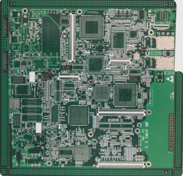
The cutting of PCB boards, especially multi-layer ones, is a time-consuming and labor-intensive process that involves a lot of repetitive tasks. Designers must exercise considerable patience and attention to detail; otherwise, mistakes can easily occur. The key to effective PCB design lies in utilizing suitable software to automate repetitive tasks, which not only saves time but also ensures precision.
1. A scanner is essential during the cutting process.
Many designers have a habit of drawing directly within PCB design software like PROTEL, PADSOR, or CAD. This practice is not advisable. The scanned graphic file serves as both the foundation for converting into a PCB file and as a reference for subsequent inspections. Using scanners can significantly reduce the difficulty and intensity of labor. It’s not an exaggeration to state that with proper scanner utilization, even those without design experience can successfully complete PCB board cutting tasks.
2. Grind the board in one direction.
In the interest of speed, some designers opt for bi-directional grinding (i.e., grinding the board layers from both the front and rear surfaces towards the middle). This approach is fundamentally flawed. Bi-directional grinding can easily wear through the layers, leading to damage in other areas, with predictable consequences. The outer layer of a PCB is the hardest due to its materials and processes, such as copper foil and pads, while the middle layer is the softest. Consequently, issues are more pronounced in the intermediate layers, often rendering them impossible to polish adequately. Additionally, the materials, hardness, and elasticity of PCBs from different manufacturers vary, making precise grinding challenging.
3. Choose high-quality conversion software.
The conversion of scanned graphic files into PCB files is crucial to the entire process. A reliable conversion tool is essential. With good conversion software, designers can efficiently “capture the essence and reproduce the design,” merely tracing the graphics once to complete the task. I recommend EDA2000, as it truly streamlines the process.
If you have any PCB manufacturing needs, please do not hesitate to contact me.Contact me

