PCB Engineering Design Requirements
- According to industry standards, the size of the single-sided solder mask should be 0.05mm larger than the flux pad to avoid covering the flux layer.
- The width of the one-sided solder mask is crucial for production and processing requirements.
- Optimizing the design for chip pins can improve the solder resist bridge process.
Impact of Improper PCB Soldering Design
- Actual Soldering Effect: Defect rates exceeding 50% and short-circuited chip pins are common outcomes.
- Thermal cycle tests reveal additional defects, affecting the functionality of the PCB.
Optimization for PCBA Manufacturing Process
Research and optimization play a crucial role in improving PCB solder mask design and PCBA manufacturability.
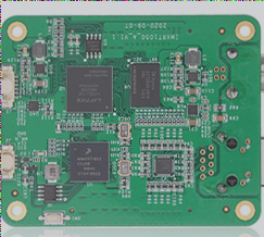
Key Points:
- Referring to industry standards like IPC 7351 for package libraries can guide optimal solder pad and mask designs.
- Increasing spacing between pads and masks reduces the risk of poor soldering quality.
- Adjusting pad widths and mask sizes ensures compatibility with PCB processing requirements.
Design Verification Process:
- Optimizing pad and mask designs improves edge spacing, meeting solder mask process requirements.
- Testing the redesigned PCBs confirms the effectiveness of the optimization scheme.
Conclusion:
The optimized design enhances product reliability and meets the necessary manufacturability standards for PCB solder mask design and PCBA assembly.
Improving PCB Design for Chips with Device Pin Edge Spacing Less than 0.2mm
When dealing with chips that have a device pin edge spacing of less than 0.2mm, traditional packaging designs may not suffice. It is essential to make adjustments in the PCB layout design to ensure the reliability of the soldering contact area.
- Adjust the width and length of the soldering pad to enhance soldering reliability.
- Remove excess copper if the solder pad is too large or the distance between solder mask edges is too small.
- Optimize the solder mask design to increase the edge width of the two solder masks for effective PCBA welding.
The interplay between soldering flux and solder mask pad design plays a critical role in enhancing PCBA manufacturability and boosting soldering yield rates.
If you require PCB manufacturing services tailored to these specifications, feel free to contact me.

