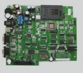
1. As an indispensable part of electronic products, printed circuit boards (PCBs) play a crucial role in realizing their functions. This underscores the growing significance of PCB design, as its performance directly impacts the functionality and cost of electronic products. Superior PCB design helps avoid numerous issues, ensuring smooth production and meeting all practical application needs.
2. PCB Manufacturability
3. The integration of manufacturability and PCB design is essential for achieving efficient manufacturing, high quality, and cost-effectiveness. PCB manufacturability research encompasses a broad range of topics, typically categorized into PCB manufacturing and PCB assembly.
4. PCB Production
5. In PCB manufacturing, several factors must be considered: PCB size, shape, process edges, and mark points. If these factors are not fully addressed during the PCB design phase, the automatic chip placement machine may struggle with the prefabricated PCB boards, potentially necessitating additional processing steps. In the worst case, some boards may require manual soldering, leading to longer manufacturing cycles and increased labor costs.
6. PCB Size

Here is the revised version of your article:
—
**01. PCB Size**
Each chip mounter has specific PCB size requirements, which vary based on the parameters of the mounter. For instance, the maximum PCB size accepted by the chip mounter is 500mm x 450mm, and the minimum size is 30mm x 30mm. This does not mean that components smaller than 30mm x 30mm cannot be handled; smaller sizes can be managed with jigsaw methods. However, when only manual installation is required, and labor costs rise or production cycles are uncontrollable, chip placement machines cannot accommodate PCB boards that are excessively large or small. Therefore, during the PCB design stage, it is crucial to fully consider the size requirements set by automatic installation and manufacturing, keeping them within the effective range.
**02. PCB Shape**
Besides size, chip placement machines also have shape requirements for PCBs. Typically, the PCB shape should be rectangular, with a length-to-width ratio of 4:3 or 5:4 (preferable). Irregular PCB shapes necessitate additional measures before SMT assembly, leading to increased costs. To avoid this, design the PCB into a standard shape during the design stage to meet SMT requirements. If the shape must be irregular, use stamp holes to achieve a normal shape in the final PCB. After assembly, redundant auxiliary baffles can be removed to meet automatic installation and space requirements.
**03. Craft Side**
To facilitate automated manufacturing, process edges must be incorporated into the PCB design to secure the board. During the design stage, a 5mm-wide process edge should be reserved, free of components and traces. The technical guide is typically placed on the short side of the PCB but can be positioned on the short side if the aspect ratio exceeds 80%. Post-assembly, the craft side used for auxiliary production can be removed.
**04. Reference Points (Mark Points)**
Mark points should be added to PCBs with installed components to ensure that assembly equipment can accurately determine component locations. Thus, mark points are essential for SMT manufacturing. Components require 2 mark points, while PCBs need 3. These should be placed on the PCB’s edge and cover all SMT components, with a minimum center distance of 5mm from the edge. For double-sided SMT components, mark points should be on both sides. If components are too densely packed, place the mark points on the process edge.
**PCB Assembly**
PCB assembly, or PCBA, involves soldering components onto a bare board. To meet automated manufacturing requirements, PCB assembly imposes specific standards for component packaging and layout.
**01. Component Packaging**
In the PCBA design phase, improper component packaging and insufficient spacing can prevent automatic installation. To achieve optimal component packaging, use professional EDA design software compatible with international standards. Ensure that the bird’s-eye view area does not overlap with other areas, allowing automatic IC placement machines to accurately identify and mount components.
**02. Component Layout**
Component layout is crucial as it affects PCB appearance and manufacturing complexity. During layout, determine the assembly surface for SMD and THD components, with the front side of the PCB as component A and the back as component B. The layout should consider various assembly forms, such as single-layer or double-layer packaging, and mixed packaging on A-side or B-side. Choose the layout that simplifies manufacturing and enhances efficiency. Additionally, maintain consistent component orientation, spacing, heat dissipation, and component height. Component orientation should align with polarity marks, and components without polarity should be arranged on the X or Y axis. Maintain a maximum height of 4mm, and keep component and PCB transmission directions at 90°. Ensure consistent spacing between components, with components in the same network close together and safe distances between different networks to account for voltage drop. The silk screen and pad must not overlap to avoid installation issues. Address heat dissipation by focusing on component layout and using fans or heat sinks as needed. Place high components behind lower ones and keep heat-sensitive components away from heat sources.
2. PCB Manufacturability
3. The integration of manufacturability and PCB design is essential for achieving efficient manufacturing, high quality, and cost-effectiveness. PCB manufacturability research encompasses a broad range of topics, typically categorized into PCB manufacturing and PCB assembly.
4. PCB Production
5. In PCB manufacturing, several factors must be considered: PCB size, shape, process edges, and mark points. If these factors are not fully addressed during the PCB design phase, the automatic chip placement machine may struggle with the prefabricated PCB boards, potentially necessitating additional processing steps. In the worst case, some boards may require manual soldering, leading to longer manufacturing cycles and increased labor costs.
6. PCB Size

Here is the revised version of your article:
—
**01. PCB Size**
Each chip mounter has specific PCB size requirements, which vary based on the parameters of the mounter. For instance, the maximum PCB size accepted by the chip mounter is 500mm x 450mm, and the minimum size is 30mm x 30mm. This does not mean that components smaller than 30mm x 30mm cannot be handled; smaller sizes can be managed with jigsaw methods. However, when only manual installation is required, and labor costs rise or production cycles are uncontrollable, chip placement machines cannot accommodate PCB boards that are excessively large or small. Therefore, during the PCB design stage, it is crucial to fully consider the size requirements set by automatic installation and manufacturing, keeping them within the effective range.
**02. PCB Shape**
Besides size, chip placement machines also have shape requirements for PCBs. Typically, the PCB shape should be rectangular, with a length-to-width ratio of 4:3 or 5:4 (preferable). Irregular PCB shapes necessitate additional measures before SMT assembly, leading to increased costs. To avoid this, design the PCB into a standard shape during the design stage to meet SMT requirements. If the shape must be irregular, use stamp holes to achieve a normal shape in the final PCB. After assembly, redundant auxiliary baffles can be removed to meet automatic installation and space requirements.
**03. Craft Side**
To facilitate automated manufacturing, process edges must be incorporated into the PCB design to secure the board. During the design stage, a 5mm-wide process edge should be reserved, free of components and traces. The technical guide is typically placed on the short side of the PCB but can be positioned on the short side if the aspect ratio exceeds 80%. Post-assembly, the craft side used for auxiliary production can be removed.
**04. Reference Points (Mark Points)**
Mark points should be added to PCBs with installed components to ensure that assembly equipment can accurately determine component locations. Thus, mark points are essential for SMT manufacturing. Components require 2 mark points, while PCBs need 3. These should be placed on the PCB’s edge and cover all SMT components, with a minimum center distance of 5mm from the edge. For double-sided SMT components, mark points should be on both sides. If components are too densely packed, place the mark points on the process edge.
**PCB Assembly**
PCB assembly, or PCBA, involves soldering components onto a bare board. To meet automated manufacturing requirements, PCB assembly imposes specific standards for component packaging and layout.
**01. Component Packaging**
In the PCBA design phase, improper component packaging and insufficient spacing can prevent automatic installation. To achieve optimal component packaging, use professional EDA design software compatible with international standards. Ensure that the bird’s-eye view area does not overlap with other areas, allowing automatic IC placement machines to accurately identify and mount components.
**02. Component Layout**
Component layout is crucial as it affects PCB appearance and manufacturing complexity. During layout, determine the assembly surface for SMD and THD components, with the front side of the PCB as component A and the back as component B. The layout should consider various assembly forms, such as single-layer or double-layer packaging, and mixed packaging on A-side or B-side. Choose the layout that simplifies manufacturing and enhances efficiency. Additionally, maintain consistent component orientation, spacing, heat dissipation, and component height. Component orientation should align with polarity marks, and components without polarity should be arranged on the X or Y axis. Maintain a maximum height of 4mm, and keep component and PCB transmission directions at 90°. Ensure consistent spacing between components, with components in the same network close together and safe distances between different networks to account for voltage drop. The silk screen and pad must not overlap to avoid installation issues. Address heat dissipation by focusing on component layout and using fans or heat sinks as needed. Place high components behind lower ones and keep heat-sensitive components away from heat sources.

