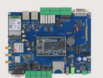
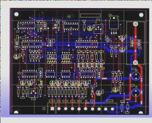
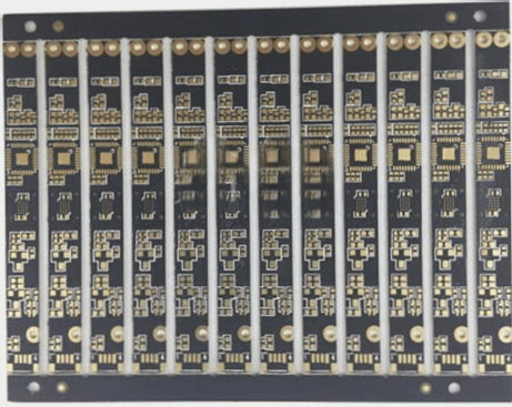
Qualified Standards for PCB Copy Boards:
**1. Disconnection:**
A. A break or discontinuity exists in the trace.
B. The cable length exceeds 10mm and is beyond repair.
C. The disconnection is located near a pad or hole edge. (If the gap is ≤ 2mm, it can be repaired at the pad or edge. If the distance between the break and the pad or hole flange is > 2mm, it cannot be repaired.)
D. Adjacent traces cannot be repaired by side disconnections.
E. The trace is disconnected at a corner. (If the break is ≤ 2mm at the corner, it can be repaired. If the break exceeds 2mm at the corner, it cannot be repaired.)
**2. Short Circuit:**
A. A short circuit caused by a foreign object between two traces, which is repairable.

B. The inner short circuit cannot be repaired.
3. Line gap,
A. If the line gap is less than 20% of the original line width, it can be repaired.
4. Line SAG and indentation,
A. If the line is uneven or the line pressure has dropped, it can be repaired.
5. The thread is dyed with tin,
A. If the wire is dipped in tin (with a total tin area of less than or equal to mm²), it can be repaired; if the tin area exceeds mm², it cannot be repaired.
6. Poor line maintenance,
A. If the complement code offset or specification does not meet the original line size (without affecting the minimum width or spacing), it can be repaired.
7. The wire is exposed to copper,
A. PCB solder wire exposure can be repaired.
8. The line is crooked,
A. If the spacing is smaller than the original spacing or there are notches, it can be repaired.
9. Stripping,
A. If there is peeling between the copper layers, it cannot be repaired.
10. Insufficient line spacing,
A. A reduction in the double-line spacing of no more than 30% can be repaired; more than 30% cannot be repaired.
11. Copper slag,
A. The distance between two lines should not be reduced by more than 30%; it can be repaired.
B. If the two-wire component is reduced by more than 30%, it cannot be repaired.
12. Line pollution and oxidation,
A. If some lines are discolored or darkened due to oxidation or contamination, no repair is needed.
13. Underline,
A. Scratches caused by copper can be repaired, regardless of whether the copper is scratched.
14. Thin lines,
A. If the PCB line width is less than 20% of the specified width, it cannot be repaired.
**Second, the solder mask part:**
1. Color difference (standard: upper and lower level),
A. If the ink color deviates from the standard, and it’s outside the allowable range, it can be controlled using a color difference table.
2. Anti-welding cavitation;
3. Anti-welding exposed copper;
A. Green paint can be repaired by stripping copper.
4. Resistance to welding scars;
A. Solder resistance caused by scratches or substrate exposure can be repaired.
5. Solder protection on the pad,
A. Tin pads, BGA pads, and ICT pads with ink cannot be repaired.
6. Poor repair: The green paint coating area is too large or incomplete to repair; lengths greater than 30mm, areas greater than 10mm², or circles with a diameter larger than 7mm² are not repairable.
7. Contaminated by foreign objects;
A. If foreign objects are scattered in the solder mask interlayer, it can be repaired.
8. The ink is uneven;
A. Local slight ink accumulation that affects appearance does not require repair.
9. BGA Viahole Ink;
A. BGA requires 100% ink insertion.
10. CARD bus through-hole ink;
A. The through-hole of the CARD BUS connector requires 100% filling. The inspection method is to check under backlight for opacity.
11. The VIA hole is not blocked;
A. VIA holes need to be 95% blocked. The hole inspection method is backlit to check opacity.
12. Tin: no more than 30mm².
13. Pseudo exposed copper; can be repaired.
14. Wrong use of ink color; non-maintenance.
**Third, the PCB perforation part:**
1. Conce,
A. Holes blocked by foreign objects cannot be repaired.
2. Make holes,
A. Upper and lower holes caused by broken holes cannot be repaired.
B. The hole itself cannot be repaired.
3. Holes inside the green paint,
A. If a hole is covered by solder resist or white paint residue, it cannot be repaired.
4. NPTH, tin in the hole,
A. NPTH holes made from PHT holes can be repaired.
5. Kondo Lock, not applicable.
6. Leak hole lock, cannot be repaired.
7. Hole deflection or offset pads, cannot be repaired.
8. Large holes, small holes,
A. Condacon with a smaller than specified error is not repairable.
9. BGA through hole Concecy, cannot be repaired.
**Fourth, the text part:**
1. Text offset, text offset, or paint tin pad, not repairable.
2. The text color does not match, or the text color is incorrect.
3. Text replay, text shadow can be recognized and repaired.
4. Text leaks, text leaks cannot be repaired.
5. Text ink dyed board surface, repairable.
6. The text is unclear, and if it affects identification, it can be repaired.
7. The text is dropped, and if there is a tensile test with 3M 600 tape, it can be repaired.
If your have any questions about PCB ,please contact me info@wellcircuits.com
**1. Disconnection:**
A. A break or discontinuity exists in the trace.
B. The cable length exceeds 10mm and is beyond repair.
C. The disconnection is located near a pad or hole edge. (If the gap is ≤ 2mm, it can be repaired at the pad or edge. If the distance between the break and the pad or hole flange is > 2mm, it cannot be repaired.)
D. Adjacent traces cannot be repaired by side disconnections.
E. The trace is disconnected at a corner. (If the break is ≤ 2mm at the corner, it can be repaired. If the break exceeds 2mm at the corner, it cannot be repaired.)
**2. Short Circuit:**
A. A short circuit caused by a foreign object between two traces, which is repairable.

B. The inner short circuit cannot be repaired.
3. Line gap,
A. If the line gap is less than 20% of the original line width, it can be repaired.
4. Line SAG and indentation,
A. If the line is uneven or the line pressure has dropped, it can be repaired.
5. The thread is dyed with tin,
A. If the wire is dipped in tin (with a total tin area of less than or equal to mm²), it can be repaired; if the tin area exceeds mm², it cannot be repaired.
6. Poor line maintenance,
A. If the complement code offset or specification does not meet the original line size (without affecting the minimum width or spacing), it can be repaired.
7. The wire is exposed to copper,
A. PCB solder wire exposure can be repaired.
8. The line is crooked,
A. If the spacing is smaller than the original spacing or there are notches, it can be repaired.
9. Stripping,
A. If there is peeling between the copper layers, it cannot be repaired.
10. Insufficient line spacing,
A. A reduction in the double-line spacing of no more than 30% can be repaired; more than 30% cannot be repaired.
11. Copper slag,
A. The distance between two lines should not be reduced by more than 30%; it can be repaired.
B. If the two-wire component is reduced by more than 30%, it cannot be repaired.
12. Line pollution and oxidation,
A. If some lines are discolored or darkened due to oxidation or contamination, no repair is needed.
13. Underline,
A. Scratches caused by copper can be repaired, regardless of whether the copper is scratched.
14. Thin lines,
A. If the PCB line width is less than 20% of the specified width, it cannot be repaired.
**Second, the solder mask part:**
1. Color difference (standard: upper and lower level),
A. If the ink color deviates from the standard, and it’s outside the allowable range, it can be controlled using a color difference table.
2. Anti-welding cavitation;
3. Anti-welding exposed copper;
A. Green paint can be repaired by stripping copper.
4. Resistance to welding scars;
A. Solder resistance caused by scratches or substrate exposure can be repaired.
5. Solder protection on the pad,
A. Tin pads, BGA pads, and ICT pads with ink cannot be repaired.
6. Poor repair: The green paint coating area is too large or incomplete to repair; lengths greater than 30mm, areas greater than 10mm², or circles with a diameter larger than 7mm² are not repairable.
7. Contaminated by foreign objects;
A. If foreign objects are scattered in the solder mask interlayer, it can be repaired.
8. The ink is uneven;
A. Local slight ink accumulation that affects appearance does not require repair.
9. BGA Viahole Ink;
A. BGA requires 100% ink insertion.
10. CARD bus through-hole ink;
A. The through-hole of the CARD BUS connector requires 100% filling. The inspection method is to check under backlight for opacity.
11. The VIA hole is not blocked;
A. VIA holes need to be 95% blocked. The hole inspection method is backlit to check opacity.
12. Tin: no more than 30mm².
13. Pseudo exposed copper; can be repaired.
14. Wrong use of ink color; non-maintenance.
**Third, the PCB perforation part:**
1. Conce,
A. Holes blocked by foreign objects cannot be repaired.
2. Make holes,
A. Upper and lower holes caused by broken holes cannot be repaired.
B. The hole itself cannot be repaired.
3. Holes inside the green paint,
A. If a hole is covered by solder resist or white paint residue, it cannot be repaired.
4. NPTH, tin in the hole,
A. NPTH holes made from PHT holes can be repaired.
5. Kondo Lock, not applicable.
6. Leak hole lock, cannot be repaired.
7. Hole deflection or offset pads, cannot be repaired.
8. Large holes, small holes,
A. Condacon with a smaller than specified error is not repairable.
9. BGA through hole Concecy, cannot be repaired.
**Fourth, the text part:**
1. Text offset, text offset, or paint tin pad, not repairable.
2. The text color does not match, or the text color is incorrect.
3. Text replay, text shadow can be recognized and repaired.
4. Text leaks, text leaks cannot be repaired.
5. Text ink dyed board surface, repairable.
6. The text is unclear, and if it affects identification, it can be repaired.
7. The text is dropped, and if there is a tensile test with 3M 600 tape, it can be repaired.
If your have any questions about PCB ,please contact me info@wellcircuits.com


