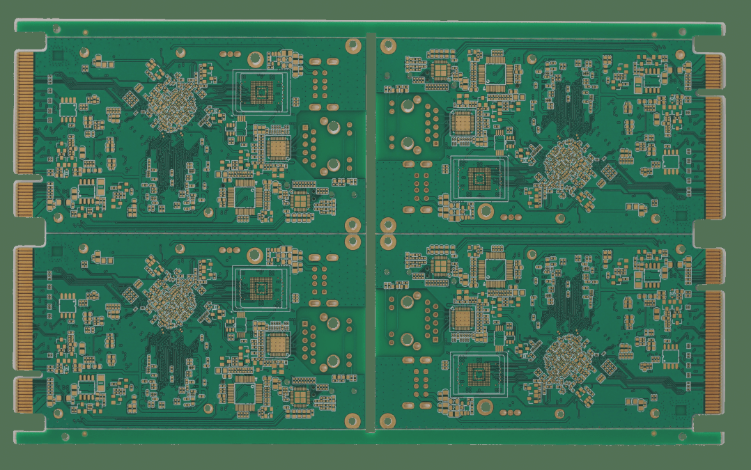
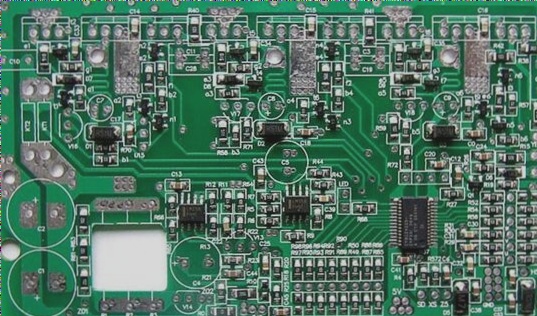
2. The small holes on the PCB are vias, which are used to connect electrical signals from one layer to another.
3. The holes on the PCB board can be roughly divided into three types: screw holes, conductive vias, and component mounting holes.

1. The screw holes are used for fixing. Conductive holes, also known as vias, function like wires to conduct electricity. Plug-in holes are used for inserting various components such as diodes, transistors, capacitors, and inductors onto the PCB. PCBs are categorized into single-sided, double-sided, and multilayer boards, with multilayer boards requiring vias to establish connections between layers. Some traces must be routed across both layers.
2. Large-area ground planes on two-layer PCBs, perforated with numerous vias, effectively reduce noise and cushion circuit board deformation. Vias connect electrical signals between different layers. Moreover, vias serve to reduce parasitic capacitance between copper layers, thereby enhancing conduction efficiency.
3. PCB holes are classified as PTH (plated through-hole) and NPTH (non-plated through-hole). PTHs facilitate electrical connections between layers after copper immersion, linking first and second layer circuits. Non-conductive holes include positioning holes and component plug-in holes.
PCB Prototyping: Electroless Nickel-Gold Immersion (ENIG)
Electroless Nickel-Gold Immersion (ENIG) coating is widely adopted for PCBs, despite its higher unit cost, due to its flat surface and excellent solderability. However, the electroless nickel layer is fragile and prone to “black pad” or “mud cracking” under mechanical stress, which has led to criticism within the industry. Benefits include reliable solder joints, a flat surface conducive to multiple reflow solderings, and a long storage life. Drawbacks include high costs (approximately five times that of HASL) and the use of chemicals like cyanide in the manufacturing process.
PCB Prototyping: Silver Immersion
Silver immersion, a newly introduced PCB surface treatment method primarily used in Asia, is gaining traction in North America and Europe. During soldering, the silver layer alloys with tin/lead, forming a robust joint ideal for BGA packages. Its distinct color aids inspection and provides a natural alternative to HASL for soldering. Despite its promising prospects, silver immersion is viewed cautiously by end-users and manufacturers alike, positioning it as an emerging lead-free surface treatment option.
—
This revision aims to maintain the original content and structure while enhancing clarity and readability.


