Acceptance Standards for PCB Circuit Boards
PCB, the essential electronic material in PCBA processing, plays a crucial role in every PCBA process. When accepting a PCBA circuit board, it is important to consider various acceptance standards and criteria for assessment.
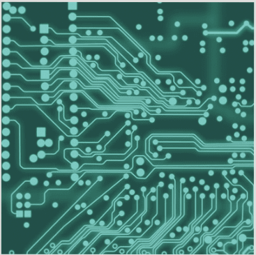
Surface Characteristics Inspection
- Sheet edges and surface defects include burrs, gaps, scratches, grooves, fiber scratches, exposed fabrics, voids, foreign inclusions, white spots, layering, pink circles, and laminated voids.
- Plated through holes should be checked for misalignment, foreign inclusions, and plating or coating defects.
- Printed contact piece inspection involves looking for pits, pinholes, nodulation, and exposed copper.
- Graphic size assessment covers size, thickness, aperture, and graphic accuracy.
- Additional considerations include wire width and spacing, coincidence, ring width, and the flatness of the printed circuit board.
PCB Board Edge Defects
Defects such as burrs, gaps, and halos along the board’s edge require specific acceptance criteria:
Burrs
- Ideal: Smooth and burr-free edge.
- Acceptable: Rough edge without damage.
- Rejection: Severely damaged edge.
Gap
- Ideal: Smooth edges without gaps.
- Acceptable: Rough edges with no defects; notch depth within specified limits.
- Reject: Fails to meet standards.
Halo
A halo refers to conductive fragmentation or delamination on or beneath the substrate’s surface due to machining:
- Ideal: No halo present.
- Acceptable: Halo within specified limits.
- Reject: Fails to meet standards.
Laminated Substrate
Defects such as weave reveal, breakage, and fiber breakage may be present:
- Exposed Fabric: Acceptable if minimum wire spacing requirements are met.
- Significant Cloth Pattern: Visible patterns are acceptable.
- Exposed Fiber/Fiber Break: Acceptable if spacing requirements are maintained.
Pits and Holes
- Ideal: No pits or holes present.
- Acceptable: Limited pit or void sizes with specific conditions.
- Reject: Fails to meet standards.
Leukoplakia and Microcrack
White spots and microcracks are internal defects related to thermal and mechanical stress, respectively.
- White spots are acceptable except in high-voltage applications.
- Microcracks are visible as white dots and should be monitored.

PCB Quality Standards
When it comes to PCB quality standards, certain criteria must be met to ensure the reliability and functionality of printed circuit boards. Here are some important points to consider:
Microcracks Tolerance
- Microcracks reducing wire spacing below minimum values may be accepted, as long as they do not exceed 50% of the distance between conductive patterns. Microcracks at the board edge should not impact the minimum distance from the edge (typically 2.5mm). If defects do not worsen after thermal stress testing, 2nd and 3rd grade boards may be deemed acceptable.
- If microcracks exceed 50% of conductive pattern spacing without causing bridging, level 1 boards may be accepted, provided other conditions remain unchanged.
Delamination and Blistering Criteria
Delamination and blistering are critical issues that affect the integrity of PCBs. Acceptance criteria per IPC-A-600G for Class 2 and 3 boards include:
- The affected area by defects should not exceed 1% of each side’s area.
- Defects must not reduce spacing below specified minimums.
- Blistering or delamination spans must not exceed 25% of the distance between adjacent conductive patterns.
- Defects should not expand post-thermal stress testing.
- The distance from the board edge must meet minimum distance requirements, typically over 2.5mm.
For Class 1 boards, the acceptance conditions are slightly different:
- The defect area cannot exceed 1% of each side’s area.
- Blistering or delamination must not exceed 25% of adjacent wire spacing, without going below the minimum spacing.
- Defects should not expand post-thermal stress testing.
- The distance from the board edge must meet or exceed the minimum distance requirements, usually greater than 2.5mm.
Foreign Inclusions Guidelines
Foreign inclusions, whether metal or non-metallic particles, can impact PCB performance. Here are some guidelines:
- The distance to the nearest conductor from foreign inclusions should be at least 0.125mm.
- Foreign inclusions must not reduce the distance between adjacent wires below the minimum requirements, typically 0.125mm unless specified otherwise.
- The electrical performance of the board should not be compromised by foreign inclusions.
Feel free to reach out if you require further adjustments!