Common Mistakes in PCB Design and Manufacturing
1. Common Mistakes in the Schematic Diagram of a PCB
- (1) Issue: Pin has no access signal
- a. Ensure I/O attributes are defined for pins
- b. Check pin direction when creating components
- c. Watch for inconsistent net properties
- The absence of engineering documentation is a common reason for this error, especially among beginners.
- (2) Issue: PCB component extends outside drawing boundary
- (3) Issue: Avoid using table names in multi-part component creation
- (4) Issue: Project file netlist not fully adjusted to PCB
2. Common Mistakes in PCB Design
- (1) Issue: NODE not found during network loading
- a. Check components in the schematic against PCB library
- b. Ensure consistent naming in the schematic and PCB library
- c. Verify components match between schematic and PCB
- (2) Issue: Printing errors
- a. Check PCB library location
- b. Avoid moving components excessively
- (3) Issue: Network divided into parts (DRC reports)
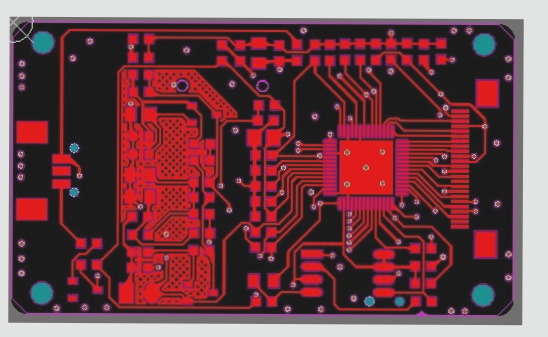
3. Common Mistakes in PCB Manufacturing
Shenzhen Zhongke Circuit Technology Co., Ltd., a leading PCB supplier, offers insights on integrating PCB design and manufacturing:
- (1) Pad Overlap
- a. Overlapping pads can cause drilling issues
- b. Improper isolation in multi-layer boards
- (2) Irregular Use of Graphic Layers
- a. Avoid placing design elements on incorrect layers
- b. Minimize unnecessary design elements
- (3) Unreasonable Use of Text
- a. Avoid text overlapping with SMD pads
- b. Use standard font sizes for clarity
- (4) Single-Sided Pad with Drilling Hole
- a. Set hole diameter to zero if drilling not required
- b. Ensure correct treatment of single-sided pads
- (5) Pads with Padding Edge Blocks
- (6) Designing Cooling Plates and Signal Lines on the Same Layer
- (7) Excessively Small Grid Spacing
- (8) Graphics Too Close to the Outer Frame
PCB Design Tips for Optimal Performance
- Ensure a minimum spacing of 0.2 mm from the graphics to the outer edge (0.35 mm if using V-shaped cutting). Insufficient spacing can cause copper foil lifting on the outer layer and affect flux flow, degrading appearance quality (including copper layers in multi-layer boards).
- Unclear Frame Design
Inconsistent or excessive design layers for the frame can confuse PCB manufacturers, making it difficult to determine the proper formation. The standard frame should be placed on the mechanical or BOARD layer, with a clear internal void. - Uneven Graphic Design
Uneven current distribution during pattern plating can lead to non-uniform coating and may cause warpage of the PCB. - Short Special Holes
The length-to-width ratio of special holes should be 2:1, with a minimum width of 1.0 mm. Otherwise, CNC drilling may not be feasible. - Lack of Designed Milling Positioning Holes
It is advisable to design at least two positioning holes with a diameter of 1.5 mm on the PCB. - Unclear Aperture Marks
- Group similar holes together in a common area to minimize complexity.
- Aperture sizes should be marked in the metric system, with a tolerance of +0.05 mm.
- Ensure that the tolerances for metallized holes and special holes (such as crimp holes) are clearly indicated.
- Unreasonable Design of Inner Layers in Multi-Layer PCBs
- Gaps in the isolation zone can lead to confusion during manufacturing.
- An isolation zone that is too narrow may make network identification difficult.
- Placing thermal pads on spacers may cause poor connections due to hole misalignment.
If you have any questions about PCB design, please feel free to contact us at info@wellcircuits.com.