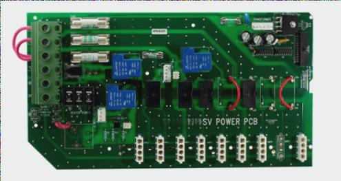
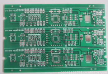
Common Issues with PCB Copy Boards
-
Unreasonable Character Placement
1. SMD soldering pads under character cover pads can hinder component soldering and circuit board testing.
2. Small characters complicate screen printing, while large characters may overlap and be hard to read.
-
Lack of Clarity in PCB Processing
1. Lack of explanation for single-sided boards can lead to poor soldering quality.
2. Processing multilayer boards out of order can cause confusion.
-
Drawing Pads with Filler Blocks
Pads with filler blocks can pass DRC inspections but complicate solder mask data generation.
-
Setting Aperture for Single-Sided Pads
Drilling requirements for single-sided pads must be clearly indicated to avoid issues.
-
Stacking of Pads
Repeated drilling in the same location can damage the hole.
In multilayer boards, proper isolation and connection disks must be designated.
-
Misuse of the Graphics Layer
Designing circuits on incorrect layers can lead to misinterpretation and potential short circuits.
-
Electrical Ground Layer Design
All connections should be isolated to prevent short circuits.
-
Excessive Filler Blocks
Too many filler blocks or thin lines can lead to incomplete data.
-
Inadequate Spacing in Area Grids
Small gaps in grid areas can cause film breakage during manufacturing.
-
Misunderstanding Frame Design
Overlapping contour lines can create confusion during PCB production.

If you require PCB manufacturing services, feel free to contact us.