PCB Surface Finishing Techniques
Hot Air Leveling
Hot air leveling is a process that involves applying molten tin-lead solder to the PCB surface and leveling it using heated compressed air. This creates a protective coating that resists copper oxidation and ensures good solderability. The copper-tin metal compound formed during this process helps enhance the interface between the solder and copper.
Advantages of Hot Air Leveling
- Cost-effective solution for PCB surface finishing.
Shortcomings of Hot Air Leveling
- Potential issues with flatness of treated pads, especially for fine-pitch pads.
- Environmental concerns due to the use of lead in the process.
Gold-Plated Boards
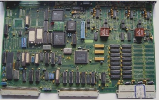
Gold plating involves applying a thin layer of real gold to the PCB surface, offering excellent conductivity and oxidation resistance. While more expensive than other methods, gold plating is commonly used for bonding, welding, and plugging applications.
Advantages of Gold-Plated Boards
- Strong conductivity and oxidation resistance.
Disadvantages of Gold-Plated Boards
- Higher costs compared to other surface finishing techniques.
- Lower welding strength in certain applications.
Chemical Gold/Immersion Gold
Chemical gold, also known as immersion gold, involves depositing a layer of gold onto the copper surface using a nickel-gold alloy. This process provides good electrical properties and long-term protection for PCBs.
Advantages of Chemical Gold/Immersion Gold
- Flat surface and good coplanarity for button contact surfaces.
- Excellent solderability with quick merging of gold with molten solder.
Disadvantages of Chemical Gold/Immersion Gold
- Complex process requiring strict parameter control.
- Risk of black pad issues leading to oxidation and compromised solder joint integrity.
Electroless Nickel Palladium Plating
Electroless nickel and palladium plating introduces a palladium layer between nickel and gold to protect against corrosion. This treatment offers reliability benefits and can be a substitute for traditional nickel-gold treatments.
Advantages of Electroless Nickel Palladium Plating
- Effective prevention of black pad defects.
Disadvantages of Electroless Nickel Palladium Plating
- Higher cost due to the scarcity of palladium.
- Strict process control requirements similar to nickel-gold treatments.
Spray Tin Circuit Board
Spray tin boards have a layer of tin sprayed onto the copper circuit, aiding in soldering. While cost-effective, they may not offer the same long-term reliability as gold-plated boards.
Advantages of Spray Tin Circuit Board
- Lower cost and good soldering performance.
Disadvantages of Spray Tin Circuit Board
- Not suitable for soldering fine gaps or very small components.
- Surface flatness inferior to gold-plated boards.
- Risk of tin bead formation leading to short circuits.

