A Guide to Thermal Relief Pads in PCB Design
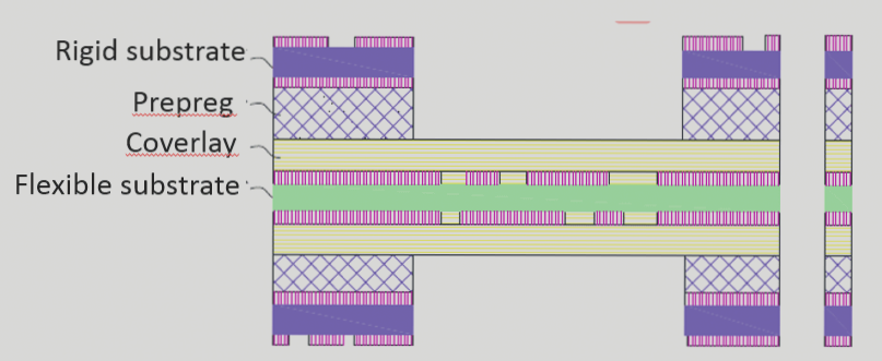
A thermal relief pad is a crucial element in PCB design that helps minimize thermal stress issues by creating a gap between the copper trace and component pin. This technique involves copper spokes extending from the pad to the surrounding copper plane, as shown in Figure 1.

Functions of Thermal Relief Pads
- Address uneven heat distribution during soldering
- Prevent overheating and potential component damage
Thermal relief pads play a crucial role in ensuring a reliable connection by directing heat effectively to the component pad. Without proper heat dissipation, soldering issues like tombstoning, cold solder joints, and solder bridging may occur.
When deciding whether to include thermal relief pads in a PCB design, consider the project’s requirements regarding high-power components, large copper pours, and soldering methods.
Considerations in Thermal Relief Pad Design
- For through-hole components, determine the appropriate pad size and shape based on component size and lead diameter.
- Consider factors like trace width, layer thickness, and copper weight when designing thermal relief pads.
- For surface-mount components, design thermal relief pads as in-via pads to ensure proper heat dissipation.
- Properly size and position the via for effective heat dissipation and maintain clearance around the pad edge.
Whether you are working with through-hole or surface-mount components, understanding the design considerations for thermal relief pads is essential to optimize heat dissipation and prevent soldering issues.
If you have any inquiries about PCBs or PCBA, don’t hesitate to reach out to us at info@wellcircuits.com.