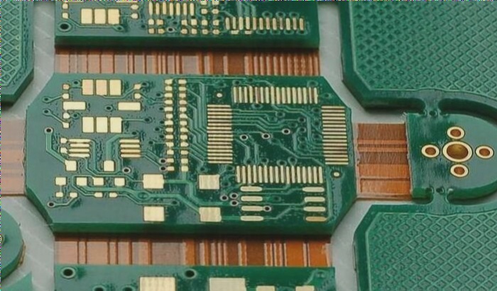
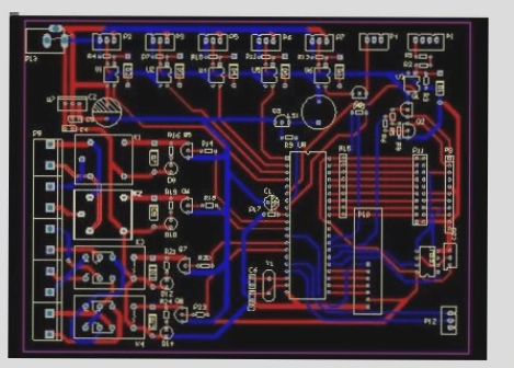
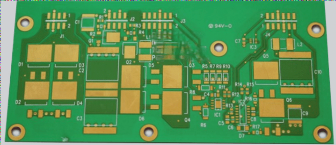
1. PCB multi-layer circuit boards are typically defined as those with 10 or more layers, often ranging from 10 to 20 or more. These boards are more complex to manufacture than traditional multi-layer boards and demand high quality and reliability.
2. They are primarily used in communication devices, high-end servers, medical electronics, aviation, industrial control, military, and other critical sectors. In recent years, the demand for advanced boards in communications, base stations, aviation, and military applications has remained robust.
3. With the rapid growth of China’s communications equipment market, the high-layer board sector holds significant promise for the future.
4. Currently, high-end PCB prototypes are predominantly produced in large volumes by foreign-invested companies or a select number of domestic manufacturers in China. The production of advanced circuit boards requires not only substantial investment in technology and equipment but also the expertise of skilled technicians and manufacturers.

At the same time, customer certification procedures for multilayer circuit boards are becoming more stringent and complex. As a result, the entry barriers for high-level circuit boards into the market are significant, and the industrial production cycle is lengthy.
The overall performance of PCBs has become an important technical indicator for assessing the capabilities and product portfolio of PCB manufacturers. This article briefly highlights the main production challenges encountered in the fabrication of advanced circuit boards, and outlines key production technology control points for multilayer boards, for reference. Compared to traditional PCB products, advanced PCBs feature characteristics such as thicker substrates, multiple layers, dense traces, numerous via holes, large unit sizes, and thin middle layers. These attributes demand greater internal space, precise layer alignment, impedance control, and enhanced reliability.
### PCB Multilayer Board Production
**1: Layer Alignment Challenges**
Given the large number of inner layers, users increasingly demand precise calibration of the PCB stack-up. Typically, the alignment tolerance between layers is controlled within 75 microns. Considering the large size of high-layer-count boards, the high temperature and humidity in the imaging environment, and misalignments caused by variations in core materials or positioning methods between layers, controlling these factors becomes increasingly challenging in high-layer boards.
**2: Challenges in Internal Circuit Fabrication**
Advanced PCBs often use special materials such as high-TG (glass transition temperature) laminates, high-speed and high-frequency materials, thick copper, and thin dielectric layers. These materials introduce stringent requirements for internal circuit manufacturing and pattern control. For example, ensuring signal integrity in impedance transmission adds complexity to the internal circuit production. Narrow trace widths and small spacing between lines increase the risk of open circuits and short circuits, leading to a higher rate of failure. Fine-line signal layers are prone to detection errors during internal AOI (Automated Optical Inspection), while thin core materials are susceptible to issues like wrinkling, poor exposure, and curling during the etching process. Advanced PCBs also feature larger system boards, resulting in higher product scrap costs.
**3: Compression of PCB Manufacturing Complexity**
The stacking of multiple inner core layers and pre-pregs (semi-cured laminates) during PCB fabrication increases the likelihood of defects such as plate shifting, delamination, resin voids, and bubble residues during the lamination process. In designing the laminate structure, it is crucial to fully consider factors such as material heat resistance, pressure resistance, resin content, and dielectric thickness. A well-planned high-layer laminate strategy is essential to avoid these issues. Given the large number of layers, achieving consistent expansion, contraction, and dimensional stability across all layers is difficult. Thin insulating layers, in particular, can result in failure during interlayer reliability tests.
**4: Drilling Challenges**
The use of specialized materials such as high-TG, high-speed, high-frequency, and thick copper substrates increases the difficulty of PCB drilling, leading to rougher drill holes and more burrs. With numerous layers and increased copper and substrate thickness, drill bits are more prone to breakage. The presence of compact BGAs (Ball Grid Arrays) and narrow hole-to-hole spacing also increases the risk of CAF (Conductive Anodic Filament) failures. Additionally, thicker boards may lead to issues with drilling alignment, making precise drilling even more challenging.
If your have any questions about PCB ,please contact me info@wellcircuits.com
2. They are primarily used in communication devices, high-end servers, medical electronics, aviation, industrial control, military, and other critical sectors. In recent years, the demand for advanced boards in communications, base stations, aviation, and military applications has remained robust.
3. With the rapid growth of China’s communications equipment market, the high-layer board sector holds significant promise for the future.
4. Currently, high-end PCB prototypes are predominantly produced in large volumes by foreign-invested companies or a select number of domestic manufacturers in China. The production of advanced circuit boards requires not only substantial investment in technology and equipment but also the expertise of skilled technicians and manufacturers.
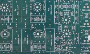
At the same time, customer certification procedures for multilayer circuit boards are becoming more stringent and complex. As a result, the entry barriers for high-level circuit boards into the market are significant, and the industrial production cycle is lengthy.
The overall performance of PCBs has become an important technical indicator for assessing the capabilities and product portfolio of PCB manufacturers. This article briefly highlights the main production challenges encountered in the fabrication of advanced circuit boards, and outlines key production technology control points for multilayer boards, for reference. Compared to traditional PCB products, advanced PCBs feature characteristics such as thicker substrates, multiple layers, dense traces, numerous via holes, large unit sizes, and thin middle layers. These attributes demand greater internal space, precise layer alignment, impedance control, and enhanced reliability.
### PCB Multilayer Board Production
**1: Layer Alignment Challenges**
Given the large number of inner layers, users increasingly demand precise calibration of the PCB stack-up. Typically, the alignment tolerance between layers is controlled within 75 microns. Considering the large size of high-layer-count boards, the high temperature and humidity in the imaging environment, and misalignments caused by variations in core materials or positioning methods between layers, controlling these factors becomes increasingly challenging in high-layer boards.
**2: Challenges in Internal Circuit Fabrication**
Advanced PCBs often use special materials such as high-TG (glass transition temperature) laminates, high-speed and high-frequency materials, thick copper, and thin dielectric layers. These materials introduce stringent requirements for internal circuit manufacturing and pattern control. For example, ensuring signal integrity in impedance transmission adds complexity to the internal circuit production. Narrow trace widths and small spacing between lines increase the risk of open circuits and short circuits, leading to a higher rate of failure. Fine-line signal layers are prone to detection errors during internal AOI (Automated Optical Inspection), while thin core materials are susceptible to issues like wrinkling, poor exposure, and curling during the etching process. Advanced PCBs also feature larger system boards, resulting in higher product scrap costs.
**3: Compression of PCB Manufacturing Complexity**
The stacking of multiple inner core layers and pre-pregs (semi-cured laminates) during PCB fabrication increases the likelihood of defects such as plate shifting, delamination, resin voids, and bubble residues during the lamination process. In designing the laminate structure, it is crucial to fully consider factors such as material heat resistance, pressure resistance, resin content, and dielectric thickness. A well-planned high-layer laminate strategy is essential to avoid these issues. Given the large number of layers, achieving consistent expansion, contraction, and dimensional stability across all layers is difficult. Thin insulating layers, in particular, can result in failure during interlayer reliability tests.
**4: Drilling Challenges**
The use of specialized materials such as high-TG, high-speed, high-frequency, and thick copper substrates increases the difficulty of PCB drilling, leading to rougher drill holes and more burrs. With numerous layers and increased copper and substrate thickness, drill bits are more prone to breakage. The presence of compact BGAs (Ball Grid Arrays) and narrow hole-to-hole spacing also increases the risk of CAF (Conductive Anodic Filament) failures. Additionally, thicker boards may lead to issues with drilling alignment, making precise drilling even more challenging.
If your have any questions about PCB ,please contact me info@wellcircuits.com

