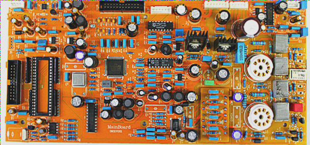
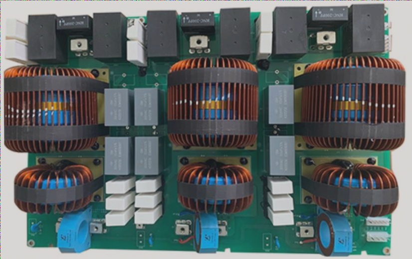
1. Layout refers to the careful placement of components on the PCB, taking into account various factors such as signal integrity, EMC, thermal management, DFM, DFT, structural requirements, and safety regulations. In high-speed PCB design, achieving a well-organized layout is the essential first step toward a successful PCB.
2. What is the concept of PCB design layout?
3. In the PCB layout process, the initial consideration is the size of the board. Next, attention must be given to components and areas that have specific structural positioning requirements, including height restrictions, width limitations, and zones for punching and slotting. After that, each circuit module should be pre-laid out based on the direction of circuit signals and power flow, followed by the comprehensive placement of all components in accordance with the design principles established for each circuit module.

**Basic Principles of Layout**
1. Communicate with relevant personnel to address specific requirements regarding structure, signal integrity (SI), design for manufacturing (DFM), design for testability (DFT), and electromagnetic compatibility (EMC).
2. Based on the structural element diagram, position critical components such as connectors, mounting holes, and indicator lights, assigning them non-movable attributes and establishing their dimensions.
3. Set up no-wiring and no-layout areas in accordance with structural element diagrams and the specific needs of certain devices.
4. Consider both PCB performance and manufacturing efficiency when selecting the process flow (preferably single-sided SMT; single-sided SMT + through-hole; double-sided SMT; double-sided SMT + through-hole), and arrange layouts according to the characteristics of various processing technologies.
5. During layout, refer to the results from the pre-layout phase, following the principle of “large components first, then small; complex components first, then simple.”
6. The layout should strive to meet the following criteria: keep total wiring as short as possible, with the key signal lines being the shortest; completely separate high-voltage and high-current signals from low-voltage and low-current signals; maintain separation between analog and digital signals; isolate high-frequency signals from low-frequency ones; ensure sufficient spacing between high-frequency components. Make local adjustments while satisfying simulation and timing analysis requirements.
7. Whenever possible, adopt a symmetrical modular layout for identical circuit sections.
8. The recommended grid for layout setting is 50 mil, while a grid of 25 mil is suggested for IC device layouts. In high-density layouts, the grid for small surface mount devices should be no less than 5 mil.
**Layout Principles for Special Components**
1. Minimize wiring length between sensitive components. Avoid placing interference-prone components too close together to reduce their distribution parameters and mutual electromagnetic interference.
2. Increase the spacing between devices and wires that may have a significant potential difference to prevent accidental short circuits. High-voltage components should be located in areas not easily accessible to humans.
3. Components weighing over 15g should be secured with brackets before soldering. Large, heavy components that generate considerable heat should not be installed directly on the PCB. Instead, heat dissipation considerations should be made for their installation in the overall housing, keeping heat-sensitive components distant from heat-generating ones.
4. For adjustable components like potentiometers, adjustable inductors, variable capacitors, and micro switches, consider the structural requirements of the overall machine, including height limits, hole sizes, and center coordinates.
5. Reserve space for PCB positioning holes and fixed brackets.
**Post-Layout Checks**
In PCB design, a well-structured layout is critical for a successful outcome. After completing the layout, engineers must conduct a thorough review of the following:
1. Verify that the PCB size markings and device layout match the structural drawings and adhere to PCB manufacturing process requirements, such as minimum hole size and minimum trace width.
2. Assess potential interference between components in both two-dimensional and three-dimensional spaces, ensuring they do not conflict with the structural casing.
3. Confirm that all components have been placed appropriately.
4. Ensure that components requiring frequent insertion or replacement are easily accessible.
5. Maintain an appropriate distance between thermal devices and heating elements.
6. Check the convenience of adjusting adjustable devices and pressing buttons.
7. Ensure that the installation area for radiators is clear of obstructions.
8. Verify that the signal flow direction is optimal and that interconnections are as short as possible.
9. Consider potential line interference.
10. Ensure that plugs and sockets do not conflict with mechanical design.
2. What is the concept of PCB design layout?
3. In the PCB layout process, the initial consideration is the size of the board. Next, attention must be given to components and areas that have specific structural positioning requirements, including height restrictions, width limitations, and zones for punching and slotting. After that, each circuit module should be pre-laid out based on the direction of circuit signals and power flow, followed by the comprehensive placement of all components in accordance with the design principles established for each circuit module.

**Basic Principles of Layout**
1. Communicate with relevant personnel to address specific requirements regarding structure, signal integrity (SI), design for manufacturing (DFM), design for testability (DFT), and electromagnetic compatibility (EMC).
2. Based on the structural element diagram, position critical components such as connectors, mounting holes, and indicator lights, assigning them non-movable attributes and establishing their dimensions.
3. Set up no-wiring and no-layout areas in accordance with structural element diagrams and the specific needs of certain devices.
4. Consider both PCB performance and manufacturing efficiency when selecting the process flow (preferably single-sided SMT; single-sided SMT + through-hole; double-sided SMT; double-sided SMT + through-hole), and arrange layouts according to the characteristics of various processing technologies.
5. During layout, refer to the results from the pre-layout phase, following the principle of “large components first, then small; complex components first, then simple.”
6. The layout should strive to meet the following criteria: keep total wiring as short as possible, with the key signal lines being the shortest; completely separate high-voltage and high-current signals from low-voltage and low-current signals; maintain separation between analog and digital signals; isolate high-frequency signals from low-frequency ones; ensure sufficient spacing between high-frequency components. Make local adjustments while satisfying simulation and timing analysis requirements.
7. Whenever possible, adopt a symmetrical modular layout for identical circuit sections.
8. The recommended grid for layout setting is 50 mil, while a grid of 25 mil is suggested for IC device layouts. In high-density layouts, the grid for small surface mount devices should be no less than 5 mil.
**Layout Principles for Special Components**
1. Minimize wiring length between sensitive components. Avoid placing interference-prone components too close together to reduce their distribution parameters and mutual electromagnetic interference.
2. Increase the spacing between devices and wires that may have a significant potential difference to prevent accidental short circuits. High-voltage components should be located in areas not easily accessible to humans.
3. Components weighing over 15g should be secured with brackets before soldering. Large, heavy components that generate considerable heat should not be installed directly on the PCB. Instead, heat dissipation considerations should be made for their installation in the overall housing, keeping heat-sensitive components distant from heat-generating ones.
4. For adjustable components like potentiometers, adjustable inductors, variable capacitors, and micro switches, consider the structural requirements of the overall machine, including height limits, hole sizes, and center coordinates.
5. Reserve space for PCB positioning holes and fixed brackets.
**Post-Layout Checks**
In PCB design, a well-structured layout is critical for a successful outcome. After completing the layout, engineers must conduct a thorough review of the following:
1. Verify that the PCB size markings and device layout match the structural drawings and adhere to PCB manufacturing process requirements, such as minimum hole size and minimum trace width.
2. Assess potential interference between components in both two-dimensional and three-dimensional spaces, ensuring they do not conflict with the structural casing.
3. Confirm that all components have been placed appropriately.
4. Ensure that components requiring frequent insertion or replacement are easily accessible.
5. Maintain an appropriate distance between thermal devices and heating elements.
6. Check the convenience of adjusting adjustable devices and pressing buttons.
7. Ensure that the installation area for radiators is clear of obstructions.
8. Verify that the signal flow direction is optimal and that interconnections are as short as possible.
9. Consider potential line interference.
10. Ensure that plugs and sockets do not conflict with mechanical design.


