The essential documents required by a general circuit board assembly (PCBA) factory during the transfer process are as follows:
1. Gerber file or PCB CAD file
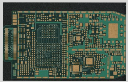
The Gerber file is the fundamental manufacturing file for PCB circuit boards. Once the PCB factory receives the Gerber file and imports it into the CAM software, it can generate production data for each PCB process. Additionally, Gerber data provides image information for specific equipment, such as automated optical inspection (AOI) systems, and serves as a reference for defining the apertures on PCB steel plates.
2. Fabrication drawing (manufacturing specifications)
This specification typically outlines the requirements for completing a circuit board, encompassing the following details. The circuit board assembly factory often relies on this specification for quality control during incoming inspections:
– The color of the insulating printing ink, which is usually green but can also be black or red.
– The color of the screen printing ink, typically white, though yellow is also used; other colors are uncommon.
– The surface finish of the printed circuit board, such as ENIG, HASL, or OSP. Some ENIG specifications include the thickness of the gold and nickel layers, and some even specify the thickness of the copper foil.

▪ The substrate grade of the circuit board. Current circuit boards are categorized into lead-free and lead-bearing processes. The temperature resistance requirements for lead-free processes are notably higher. When necessary, it is advisable to specify the Tg value (lead-free at 150°C or above) and Td value (lead-free at 325°C or above) of the FR4 substrate, as well as the Z-axis expansion coefficient (300 ppm/degree or lower).
▪ The electrical characteristics of the copper foil, particularly for high-frequency products.
▪ V-cut and additional processing or drilling details.
▪ The style and dimensions of the jigsaw puzzle. (Jigsaw/Connected boards will be covered in the next project.)
3. Panel drawing (Jigsaw/Connected board specifications)
The provided Gerber document solely defines the data for a single-chip PCB. To enhance circuit board utilization and manufacturing efficiency, the actual output is designed as a panel or connected board. The shape, style, and size of the board will influence the design of the subsequent tools, and different jigsaw methods may render the original tools unusable:
▪ Steel (Stencil)
▪ Vacuum block
▪ Parts Visual Inspection template
▪ MDA (Manufacturing Defect Analyzer) or ICT (In-Circuit Tester) test fixture
▪ FVT (Function Verification Tester)
When transitioning between various production lines and factories, it’s crucial to adhere to the original jigsaw style. If the original file does not specify the jigsaw style, you can request it from the initial circuit board manufacturer for standardization.
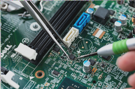
4. Placement Component X-Y table (XY coordinates of SMT parts)
The SMT printing machine determines the placement position of components on the circuit board based on user-defined X and Y coordinates. Additional parameters (Z-axis, rotation, etc.) contribute to the SMT programming. The circuit board designer can create an X, Y coordinate table for components using PCB CAD, significantly reducing the time SMT engineers spend on programming.
If generating X, Y coordinate tables from PCB CAD is not feasible, you may resort to traditional methods of manually measuring each part with a projector, or by opening the Gerber file for measurement on a computer. Regardless of the measurement method, the SMT machine will need fine-tuning to align with the actual coordinates.
5. Readable plots file (readable circuit board layer)
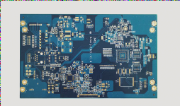
The average person may struggle to interpret Gerber files directly. Typically, we produce each layer of the PCB as a readable PDF document, encompassing the solder paste layer, silk screen layer, mask layer, and various circuit layers.
6. PCB Assembly drawing (circuit board assembly specification)
In general, today’s circuit board assembly relies on the BOM (Bill of Materials). However, there are instances where additional jumpers are required, or the BOM and part position indicators cannot provide adequate standardization. Therefore, a PCB Assembly drawing is often needed, outlining how the PCB factory can assemble the entire circuit board aside from SMT or plug-ins. This may include instructions for indicating part numbers post-assembly, additional dispensing, and other actions.
7. Schematic drawing (circuit diagram)
The schematic serves as a reference for electronic engineers or repair technicians during circuit board repairs. Circuit diagrams are sometimes utilized to design test fixtures.