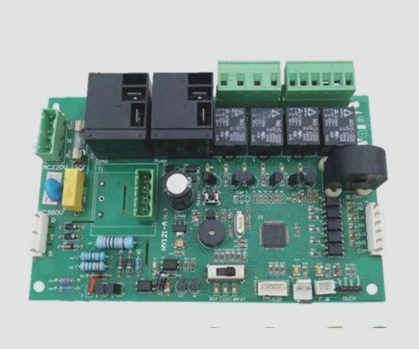
After importing the PCB board information into Protel 99SE design software, you’ll notice that the circuit board is organized into several layers, each displaying different colors and shapes within the software. Let the PCB board manufacturer give you a brief overview of the PCB layers.
1. **Signal Layer**
The signal layer is primarily utilized for routing the wires on the circuit board. Protel 99SE offers a total of 32 signal layers, which include the Top layer (top layer), Bottom layer (bottom layer), and 30 MidLayers (middle layers).
2. **Internal Plane Layer (Internal Power/Ground Layer)**
Protel 99SE provides 16 internal power and ground layers. These layers are exclusive to multilayer boards and are mainly employed for organizing power and ground lines. When we refer to double-layer, four-layer, or six-layer boards, we are indicating the total count of signal layers and internal power/ground layers.
3. Mechanical Layer
Protel 99 SE offers 16 mechanical layers, typically used to define the external dimensions of the circuit board, along with data marks, alignment marks, assembly instructions, and other mechanical details. This information varies according to the specifications of the design company or PCB manufacturer. By executing the menu command Design|Mechanical Layer, additional mechanical layers can be configured for the circuit board. Furthermore, mechanical layers can be combined with other layers for output and display purposes.
4. Solder Mask Layer
A layer of coating, such as solder resist, is applied to all areas except the pads to prevent solder from adhering to these regions. The solder mask aligns with the pads during the design phase and is generated automatically. Protel 99 SE includes two solder masks: Top Solder (top layer) and Bottom Solder (bottom layer).
5. Paste Mask Layer
This layer serves a function similar to that of the solder mask, specifically corresponding to the surface-mounted component pads during machine soldering. Protel 99 SE offers two solder paste protective layers: Top Paste (top layer) and Bottom Paste (bottom layer). It primarily applies to SMD (Surface Mount Device) components on PCBs. If only DIP (through-hole) components are used, exporting Gerber files for this layer is unnecessary. Before mounting SMD components, solder paste must be applied to each pad, and the stencil for tinning requires this Paste Mask file for processing. It’s crucial that the Gerber output for the Paste Mask layer is clear, as it mainly pertains to SMD components. Comparing this layer with the solder mask, introduced below, reveals their differing functions, even though the film images appear quite similar.
6. Keep Out Layer
This layer defines the zones where components and wiring can be effectively placed on the circuit board. A closed area is delineated on this layer to mark the effective routing zone. Automatic layout and routing cannot occur outside this designated area.
7. Silkscreen Layer
The silkscreen layer is primarily used for printed information, including the outlines and annotations of PCB components along with various text characters. Protel 99 SE features two silkscreen layers: Top Overlay and Bottom Overlay. Typically, marked characters are found on the top silkscreen layer, while the bottom layer may be closed.
8. Multi-Layer
Pads and vias on the circuit board must penetrate through the entire board to establish electrical connections with various conductive pattern layers. Consequently, the system incorporates an abstract layer known as multilayer. Generally, pads and vias should be positioned across multiple layers. If this layer is disabled, pads and vias will not be visible.
9. Drill Layer
The drilling layer supplies drilling information necessary during the PCB manufacturing process (e.g., where pads and vias require drilling). Protel 99 SE provides two drilling layers: Drill Grid (drilling indication map) and Drill Drawing (drilling schematic). In contrast, Eagle software typically has multiple layers marked in green.