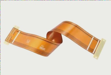
PCB assembly design involves combining a circuit board with other electronic components in order to embed them into the final product. It is crucial to consider PCB assembly during the early design phase to ensure optimal product performance and avoid manufacturing issues. Ignoring PCB assembly considerations can lead to concurrent problems that may only become apparent during the assembly stage, causing delays and performance issues. In order to avoid these mistakes, it is important to implement the following PCB assembly design skills:
- Pay attention to the gap between components to avoid potential problems caused by components being too close.
- Place components around silkscreens and assembly lines to maintain proper component spacing.
- Select good components early in the design process to prevent conflicts during assembly.
- Separate leaded components from lead-free components to ensure proper assembly standards.
- Evenly place large components to achieve optimal heat distribution during reflow soldering.
- Ensure that chip components are not too close to the edge of the PCB board, especially if V-grooves are used.
- Avoid using very small drills, unless absolutely necessary.
- Maintain sufficient clearance around mounting holes to prevent interference with connectors.
- Avoid mixing manufacturing processes as much as possible to reduce costs and assembly time.
- Select the appropriate package size for components based on available space on the PCB board.
- Find components with suitable cycle to prevent delays in the manufacturing process.
- Keep the bill of materials (BOM) up-to-date to prevent assembly issues.
- Check the component footprint to ensure proper pad patterns and dimensions.
- Ensure that indicators for all components are present to avoid polarity and orientation issues during assembly.
- Ensure that each connection of each component has its own independent pad to prevent alignment and solder deposition issues.
- Address material procurement issues to ensure that all components are supplied in a well-organized kit that matches the BOM.
- Conduct Design for Manufacturing (DFM) testing to identify and address any errors in the design at an early stage.
By implementing these PCB assembly design skills, NPI engineers can avoid DFM problems and ensure seamless PCB assembly for optimal product performance.

