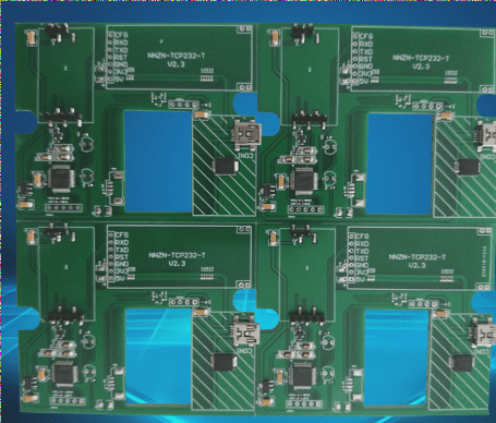
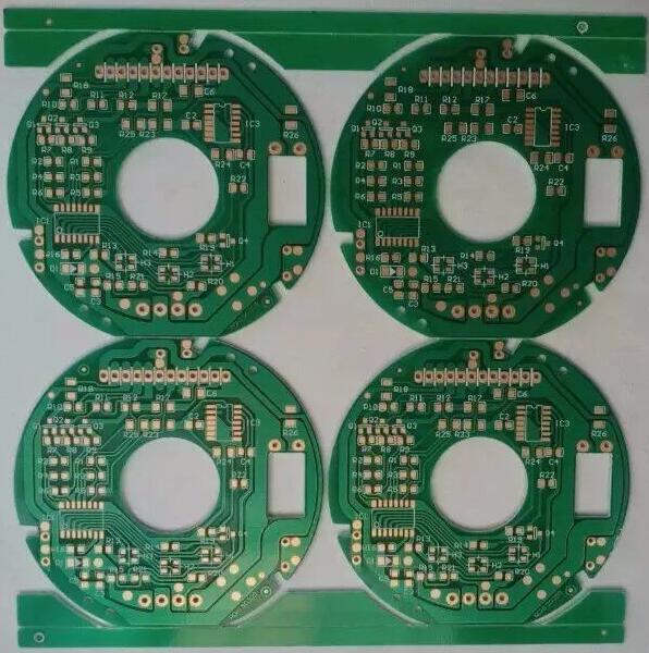
**Introduction to PCB Puzzle (Jigsaw)**
The PCB jigsaw method is primarily used for manufacturing convenience. For board manufacturers, the raw material typically comes in large sheets. They produce multiple boards simultaneously on a single sheet and then cut them into individual units. The jigsaw method is particularly beneficial when it comes to soldering production. Without this technique, imagine trying to solder a small board, roughly the size of a fingernail, one at a time on an SMT machine that’s as large as a car. The efficiency of the process would be drastically reduced, making jigsaw cutting an essential part of modern PCB production.

**PCB Jigsaw Design: Key Considerations and Best Practices**
The concept of “PCB jigsaw” can be interpreted in several ways, but the core focus is to enhance manufacturing efficiency, minimize material wastage, and ensure seamless production processes. When designed correctly, the jigsaw layout can result in both material savings and production cost reductions. However, it is crucial to understand the nuances of PCB jigsaw design to achieve optimal outcomes in production.
### 1. **Purpose of the Jigsaw Design**
A well-designed PCB jigsaw optimizes both material usage and production efficiency. For manufacturers, this means reducing material waste, while for customers, it involves meeting specific layout requirements. The convenience of the jigsaw layout lies in its ability to save material by fitting multiple small boards within a larger panel, maximizing the use of available space. For example, utilizing a 1.2m x 1m material to fit a 34cm x 41cm jigsaw is an ideal approach. This layout ensures minimal waste and maximizes the material’s utility.
### 2. **Production Efficiency Considerations**
One of the primary motivations behind PCB jigsaw design is to reduce production costs. For panels with widths between 260mm and 300mm (though this may vary depending on the production line), it’s essential to match the jigsaw layout with the capabilities of the equipment. Excessive puzzle sizes may disrupt processing speed, as each material gun is optimized to process a specific module. When the jigsaw layout exceeds the module’s processing range, the manufacturing speed will be significantly slower, thus affecting overall efficiency.
### 3. **Frame and Component Layout**
The outer frame (clamping side) of the PCB panel must be carefully designed to prevent deformation during the mounting process. It’s critical to avoid creating V-grooves along this side to maintain the panel’s integrity during fixture attachment. Regarding the component layout, it’s essential to maintain consistent orientations for all components. Mirror-imaged layouts can lead to coordinate misalignments during processing, creating significant issues during assembly.
### 4. **Edge and Connector Considerations**
The area between the PCB’s outer frame and the smaller boards should be designed without any connector extensions. These extensions can interfere with the tool’s ability to separate the boards after soldering. Additionally, the positioning of the smaller boards should maintain adequate spacing between them to facilitate easy separation during the cutting process.
### 5. **Positioning for Accurate Detection**
To ensure accurate processing, the PCB design should include at least three reference positioning points along the board’s edge. These reference points serve to establish the coordinates for the entire processing operation and ensure the board’s levelness. The positioning holes should be set at least 5mm from the edge, with the direction of travel clearly indicated to distinguish the entry direction. It’s also important to leave a non-resistance area (at least 1.5mm) around the positioning point to avoid interference from nearby pads or components.
### 6. **Positioning Holes for Each Board**
Each smaller board within the jigsaw layout must include at least three positioning holes, with a diameter between 3mm and 6mm. Additionally, there should be no traces or components within 1mm of these positioning holes to avoid misalignment during processing. Properly placed positioning holes help maintain the speed and accuracy of the assembly process, preventing later issues that may arise from improper hole placement.
### Conclusion
In summary, the primary goal of PCB jigsaw design is to reduce production costs and improve processing speed. When designing the layout, careful attention must be given to factors such as material usage, production line capabilities, panel integrity, and precise component positioning. By following these guidelines and maintaining a thoughtful design approach, manufacturers can avoid common issues, improve efficiency, and ensure a smoother production process. A well-executed jigsaw design not only saves material and reduces costs but also optimizes the overall PCB manufacturing process.
The PCB jigsaw method is primarily used for manufacturing convenience. For board manufacturers, the raw material typically comes in large sheets. They produce multiple boards simultaneously on a single sheet and then cut them into individual units. The jigsaw method is particularly beneficial when it comes to soldering production. Without this technique, imagine trying to solder a small board, roughly the size of a fingernail, one at a time on an SMT machine that’s as large as a car. The efficiency of the process would be drastically reduced, making jigsaw cutting an essential part of modern PCB production.
**PCB Jigsaw Design: Key Considerations and Best Practices**
The concept of “PCB jigsaw” can be interpreted in several ways, but the core focus is to enhance manufacturing efficiency, minimize material wastage, and ensure seamless production processes. When designed correctly, the jigsaw layout can result in both material savings and production cost reductions. However, it is crucial to understand the nuances of PCB jigsaw design to achieve optimal outcomes in production.
### 1. **Purpose of the Jigsaw Design**
A well-designed PCB jigsaw optimizes both material usage and production efficiency. For manufacturers, this means reducing material waste, while for customers, it involves meeting specific layout requirements. The convenience of the jigsaw layout lies in its ability to save material by fitting multiple small boards within a larger panel, maximizing the use of available space. For example, utilizing a 1.2m x 1m material to fit a 34cm x 41cm jigsaw is an ideal approach. This layout ensures minimal waste and maximizes the material’s utility.
### 2. **Production Efficiency Considerations**
One of the primary motivations behind PCB jigsaw design is to reduce production costs. For panels with widths between 260mm and 300mm (though this may vary depending on the production line), it’s essential to match the jigsaw layout with the capabilities of the equipment. Excessive puzzle sizes may disrupt processing speed, as each material gun is optimized to process a specific module. When the jigsaw layout exceeds the module’s processing range, the manufacturing speed will be significantly slower, thus affecting overall efficiency.
### 3. **Frame and Component Layout**
The outer frame (clamping side) of the PCB panel must be carefully designed to prevent deformation during the mounting process. It’s critical to avoid creating V-grooves along this side to maintain the panel’s integrity during fixture attachment. Regarding the component layout, it’s essential to maintain consistent orientations for all components. Mirror-imaged layouts can lead to coordinate misalignments during processing, creating significant issues during assembly.
### 4. **Edge and Connector Considerations**
The area between the PCB’s outer frame and the smaller boards should be designed without any connector extensions. These extensions can interfere with the tool’s ability to separate the boards after soldering. Additionally, the positioning of the smaller boards should maintain adequate spacing between them to facilitate easy separation during the cutting process.
### 5. **Positioning for Accurate Detection**
To ensure accurate processing, the PCB design should include at least three reference positioning points along the board’s edge. These reference points serve to establish the coordinates for the entire processing operation and ensure the board’s levelness. The positioning holes should be set at least 5mm from the edge, with the direction of travel clearly indicated to distinguish the entry direction. It’s also important to leave a non-resistance area (at least 1.5mm) around the positioning point to avoid interference from nearby pads or components.
### 6. **Positioning Holes for Each Board**
Each smaller board within the jigsaw layout must include at least three positioning holes, with a diameter between 3mm and 6mm. Additionally, there should be no traces or components within 1mm of these positioning holes to avoid misalignment during processing. Properly placed positioning holes help maintain the speed and accuracy of the assembly process, preventing later issues that may arise from improper hole placement.
### Conclusion
In summary, the primary goal of PCB jigsaw design is to reduce production costs and improve processing speed. When designing the layout, careful attention must be given to factors such as material usage, production line capabilities, panel integrity, and precise component positioning. By following these guidelines and maintaining a thoughtful design approach, manufacturers can avoid common issues, improve efficiency, and ensure a smoother production process. A well-executed jigsaw design not only saves material and reduces costs but also optimizes the overall PCB manufacturing process.