PCB is an essential component of electronic equipment, found in nearly every type of device. Besides supporting various large and small parts, the primary function of a PCB is to facilitate electrical connections between these components. Since PCBs are made from copper-clad materials, copper dumping can occur during production. Here’s a brief overview of the reasons behind this phenomenon.
1. If the PCB circuit design is poorly conceived, using thick copper foil for circuits that are too thin can lead to excessive etching and copper dumping.
2. Excessive etching of copper foil can also contribute to this issue. The electrolytic copper foils available on the market typically include single-sided galvanized (often referred to as ashing foil) and single-sided copper plating (known as red foil). Commonly, copper dumping occurs with galvanized copper foils exceeding 70µm, while red foils and ashing foils below 18µm generally do not experience significant copper dumping.
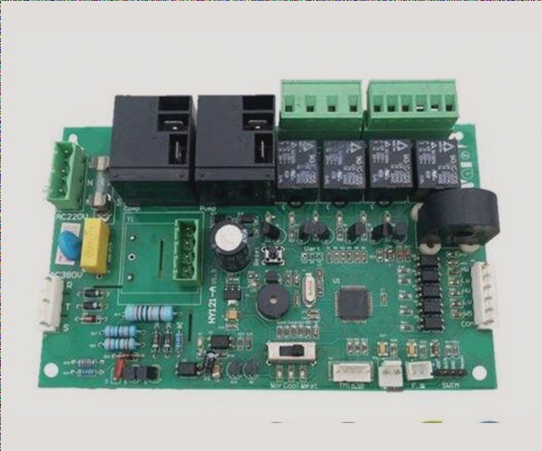
1. WellCircuits’ manufacturing facility is dedicated to offering customers a comprehensive online procurement service for electronic components. We provide access to thousands of electronic components for procurement, price inquiries, and trading, ensuring that all components are sourced from original factories or authorized agents to guarantee authenticity. We are a professional electronic components procurement platform in the domestic market.
2. During the PCB manufacturing process, local collisions can occur, causing copper wire to detach from the substrate due to external mechanical forces. This undesirable situation may result in poor positioning or directional issues; loose copper wires may exhibit noticeable distortion or show scratches/impact marks in the same direction. Examining the peeling of copper wire in problematic areas reveals that the copper foil surface appears normal, with no signs of erosion, and the peel strength of the copper foil remains intact.
3. Typically, if the laminate is pressed at high temperatures for over 30 minutes, the copper foil and the semi-cured sheet are effectively bonded. Therefore, pressing usually does not compromise the bond strength between the copper foil and substrate in the laminate. However, during the stacking process, if there is PP contamination or damage to the copper foil surface, it can lead to insufficient bonding strength post-lamination, resulting in positioning issues (particularly in large boards) or sporadic copper wire detachment. Nevertheless, there should be no abnormal copper foil peel strength near the measured area of detachment.
4. These factors contribute to copper delamination in PCBs. For those interested in learning more, please continue to follow WellCircuits; we will keep updating our knowledge to share with you.

