Challenges Faced by PCB Board Design Engineers
PCB board design engineers have encountered various challenges in recent times, which are crucial in evaluating PCB board design. Meeting these challenges and exploring potential solutions are essential aspects to consider. One example of solving PCB board design evaluation problems is through the use of Mentor’s PCB board evaluation software package.
Integrating Advanced Technology into Products
For research and development personnel, integrating advanced technology into products is a key consideration. This integration not only enhances product functions but also helps in reducing production costs. However, the challenge lies in effectively applying these technologies to products.
- Factors to Consider:
- Time-to-market: A critical factor influencing decisions around product development.
- Product Functionality: Including design implementation, testing, and EMI compliance.
- Reducing Design Iterations: Depends on the completion of previous work.

Factors Influencing PCB Board Design Decisions
When designing PCB boards, engineers must consider various factors that impact their decisions:
1. Product Functionality
- Essential functions: Interaction between schematic and PCB layout, routing capabilities, and DRC checker.
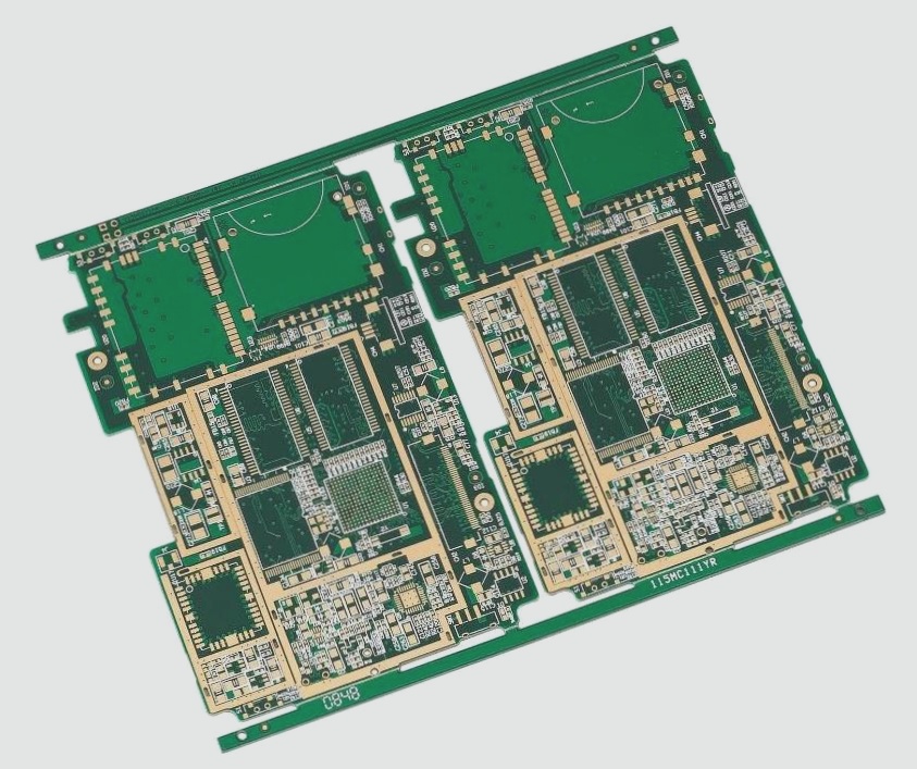
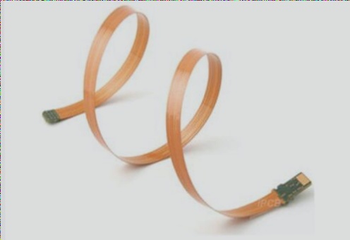
- Upgrading functionality: HDI interface, flexible design, passive components, RF design, automatic script generation, and manufacturability considerations.
2. Collaboration with Technically Proficient Partners
Having a knowledgeable partner in the industry can expedite product design with efficiency and advanced technology.
3. Considerations for PCB Board Selection
While price is a factor, prioritizing considerations such as ROI is crucial. Development tools complexity should match the design requirements, with a focus on physical routing and component placement control.
4. Exploring New Development Tool Capabilities
Designers are revisiting their development tool capabilities, looking into areas like HDI, RF design, advanced packaging, rigid-flex PCB, and signal integrity planning to enhance product design and performance.
New Developments in PCB Design
Recent advancements in parallel and differential pair structures have introduced new challenges for PCB designers. Issues like clock recovery at high frequencies, power supply noise, common-mode noise, and signal loss due to components like IC packages, PCB boards, cables, and connectors must now be carefully considered.
Enhanced Design Tools
One key aspect that can greatly benefit designers is the availability of design kits tailored to specific technologies. These kits, covering technologies such as USB, DDR/DDR2, PCI-X, PCI-Express, and RocketIO, offer comprehensive guidance on design intricacies, challenges, simulations, and routing constraints. By utilizing these design kits, designers can effectively navigate the complexities of new technologies and ensure optimal performance.
Choosing the Right PCB Tool
When venturing into new technological territories, selecting a PCB design tool is crucial. It is not just about meeting basic layout requirements but also about addressing the specific needs and challenges posed by advanced technologies. Designers should opt for tools that provide both functionality and customization options to streamline the design process and achieve desired outcomes.