Guidelines for PCB Stack Design
In the realm of PCB design, adhering to fundamental principles is crucial for optimal performance:
- Each wiring layer should have an adjacent reference layer (power or ground).
- Main power and ground layers should maintain a minimum distance for better coupling capacitance.
Stack Configurations
Here are stack configurations from a two-layer board to an eight-layer board:
- Single-sided and double-sided PCB stacking
Electromagnetic Compatibility Issues
Single and double-layer boards face increasing electromagnetic compatibility challenges. Minimizing the loop area of critical signals is essential to combat these issues.
Key Signals
Key signals, which produce strong radiation and are sensitive to external influences, play a crucial role in electromagnetic compatibility. Managing these signals effectively is vital for optimal circuit performance.
Single and Double-Layer Board Routing
For low-frequency analog designs below 10 KHz, consider the following routing guidelines:
- Route power traces radially on the same layer to minimize line length.
- Place power and ground wires close together, especially next to key signal wires, to reduce loop area and sensitivity to interference.
- On double-layer boards, route a ground wire beneath the signal wire to create the smallest loop area.
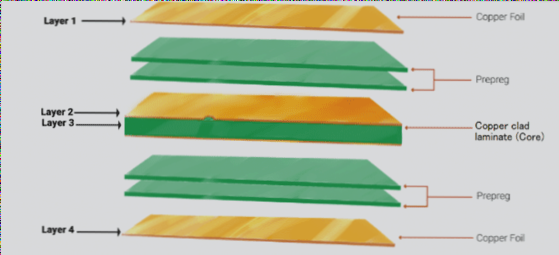
Two and Four-Layer Laminates
Consider the following laminated designs for optimal performance:
- SIG-GND(PWR)-PWR(GND)-SIG
- GND-SIG(PWR)-SIG(PWR)-GND
Optimal PCB stack design is essential for mitigating electromagnetic interference and ensuring signal integrity. By following these guidelines, you can enhance the performance and reliability of your PCB layouts.
Note:
The optimal design for PCB layouts involves separating inner signal and power mixed layers, with wiring directions oriented perpendicularly to prevent crosstalk. It is crucial to control the board area effectively to adhere to the 20H rule. To manage impedance, precise arrangement of wiring and copper placement beneath power and ground layers is vital. Interconnecting copper on power or ground layers as much as possible ensures DC and low-frequency continuity.
Latest Insights:
- Advanced PCB designs with higher chip density and clock frequencies should consider a six-layer board design for improved signal integrity.
- For the six-layer board scheme, minimizing the distance between power and ground layers is essential for optimal power and ground coupling.
- When designing PCBs, adherence to the 20H rule and mirror layer rule is crucial for successful implementation.
Stacking of Four and Eight-Layer Boards:
When selecting board layers and stacking methods in PCB design, factors such as signal networks, device density, pin density, signal frequency, and board size play a significant role.
Recommended Actions:
- For designs with more signal networks, higher device density, and increased signal frequency, multi-layer board designs are recommended.
- To enhance EMI performance, ensure each signal layer has a dedicated reference layer.
If you require PCB manufacturing services, feel free to contact us.