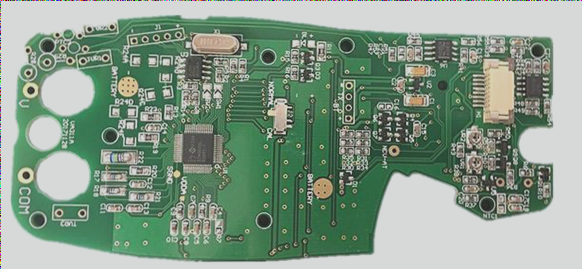
In the design and manufacturing process of multi-layer PCBs, the term “via” is frequently used. But what exactly does a via mean, and how should it be applied in designs? In this video, we will explore the basics of PCB vias.
What is a Via?
A via is a small hole drilled through two or more layers of a PCB. It allows signals and power to transfer between these layers. Since the circuits in a multi-layer PCB are independent of each other, vias are essential for creating inter-layer connections. Vias are typically classified into three types based on their functionality: blind vias, buried vias, and through-hole vias.

Figure 1. What is a Via
Types of Vias
Blind via: (From outer layer to inner layer)
A blind via starts from an outer layer (either the top or bottom) and connects to at least one inner layer, but does not pass through the entire board. As a result, blind vias are visible only on one side of the PCB. In PCB design, blind vias are often used to save space and are commonly found in BGA assembly and HDI PCBs.
Buried via: (From inner layer to inner layer)
A buried via connects two or more inner layers and is not visible from the outer layers. These vias are primarily used for inter-layer signal connections and are particularly useful in reducing signal interference, making them ideal for HDI PCBs.
Through-hole via: (From outer layer to outer layer)
The through-hole via is the most common type of via used in PCB manufacturing. It connects the inner and outer layers and passes all the way through the board. This type of via is typically used for internal connections or as mounting points for components.

Figure 2. Types of Vias
Via Covering Process
There are three main methods for covering vias: tenting vias, leaving vias uncovered, and plugging vias with solder mask.

Figure 3. Via Covering Process
Tenting vias
Tenting vias is the process of covering the via’s annular ring with a solder mask to provide insulation. It is crucial to ensure the solder mask fully covers the annular ring and is thick enough to prevent accidental short circuits or contact with other circuits.

Figure 4. Tenting Vias
Vias not covered
Choosing “vias not covered” for your PCB design means that both the via hole and its annular ring will not be covered with solder mask. This approach is typically used for debug measurement signals. Uncovered vias also have the advantage of increasing the heat dissipation area, which is beneficial for heat management. However, this method carries the risk of causing short circuits.

Figure 5. Vias Not Covered
Plugged vias with solder mask
Plugging vias with solder mask prevents solder balls from escaping during wave soldering and avoids flux residues in the via holes. This process is especially necessary when the board features BGA or IC components.

Figure 6. Vias Plugged with Solder Mask
How to Choose the Right Via for Your Design?
Unlike through-hole vias, blind and buried vias are only applicable in PCBs with at least four layers. Using blind or buried vias can effectively increase the density of multilayer PCBs, reducing the number of layers and overall board size. However, through-hole vias are easier and more cost-effective to manufacture, making them the more common choice in PCB designs.
If you have any questions about PCBs or PCBA, please feel free to contact us at info@wellcircuits.com.


