The Importance of Etching Process in PCB Manufacturing
High-Quality PCBs for Efficient Electronic Products
As a PCB expert, I know that using an etching process to expose the conductive insulation surface between wires is crucial for manufacturing printed circuit boards. High-quality PCBs are essential for developing efficient and modern electronic products. While “printed wiring board” and “printed circuit board” are often used interchangeably, they have subtle differences that are important to recognize.
Manufacturing a Printed Wiring Board
- Lamination: Involves pressing and heating substrate layers to form a laminate, providing electrical isolation for the conductive layer.
- Drilling: Essential for fixing components on the board, either manually or automatically, using specialized machines for precise holes.
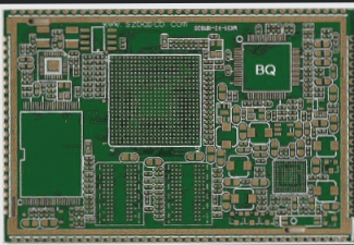
- Conductive Track Creation: Copper is commonly used for its signal transmission quality, deposited or etched to form the desired pattern.
Configurations and Materials
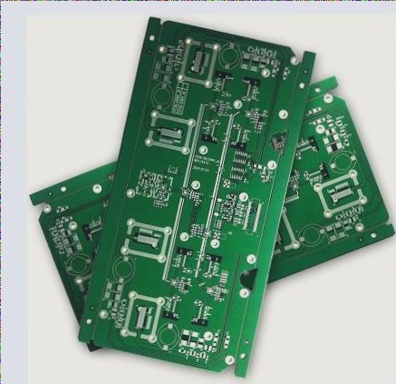
- Multiple Layers: Printed wiring boards can have surface mount and through-hole components for varied functionalities.
- Trace Materials: Copper, silver, and gold can be used based on conductivity requirements.
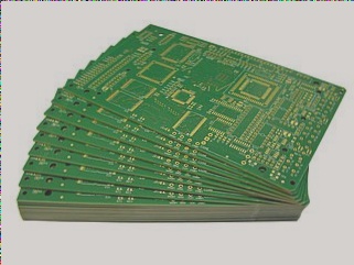
- Copper Weight: Ranges from standard to thick copper for different applications.
Conformal Coatings and Applications
- Conformal Coatings: Shield boards from external elements but may not be suitable for all printed wiring boards due to surface features.
Printed wiring boards are vital for electronic products, providing mechanical support, wiring connections, required electrical characteristics, and facilitating component installation, soldering, and maintenance for consistent quality and efficiency in manufacturing.