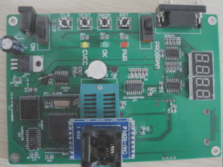
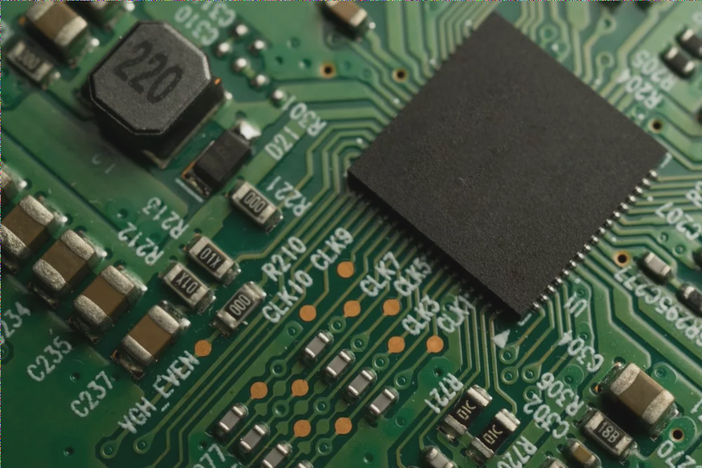
Stencil PCB is a stainless steel foil on which holes corresponding to the component pins on the surface of the PCB are laser cut. Once the PCB stencil is properly aligned on the board, solder paste (wet lead) is pulled through the stencil to fill in the holes in the stencil (this process is done only once, using a needle blade ).
The sole purpose of the PCB stencil is to transfer wet lead to the bare board. The stainless steel foil is removed from the PCB, the wet lead remains on the circuit ready to place SMD components. This process is done by machine as opposed to manual welding methods, so it ensures beauty, quality and saves time.
Depending on the thickness of the stainless steel foil and the size of the opening will control the amount of wet lead that gets into the board. Too much lead will create errors such as solder bridges, solder balls. But if there is a lack of lead, it will not be enough to create a solder joint.
The Foil Thickness of SMT stencil
The foil thickness is selected based on the types of components installed on the PCB circuit. Small packaged components, such as the 0603 capacitors or the 0.020 pitch SOIC, will require a thinner stencil than those with larger pickings like the 1206 capacitor or the 0.050 pitch SOIC. PCB stencil thickness ranges from 0.0254mm to 0.762mm. The foil thickness used on most boards is from 0.1016mm to 0.1778mm.
In the old days when through-hole components dominated electronic design, manual soldering was the way to go. With just a soldering iron and flux, it is easy to attach the component pins to the board. But today, when devices can fit in a pocket or on the wrist, through-hole components are being pushed aside by smaller competitors, SMD components.
These small components are more difficult to solder by hand, so if you have a lot of models that need to be assembled you need a more efficient way to get the components onto the board. If you are looking for a faster way to assemble all the SMD components onto the board then you need to learn about solder paste stenciling.
What is Solder Paste Stenciling?
Solder paste stenciling is the process of using the aforementioned PCB stencil to quickly apply lead cream to all the pads on the circuit. Stencil has a lot of holes corresponding to the position of the pads of the SMD arranged on the circuit.
After placing this stencil on top of the bare board, a layer of lead cream can be applied. After removing the stencil, we will have a nice, uniform layer of solder on all the pads where the SMD components are placed. In this way, it is possible to easily assemble a lot of samples quickly.
When compared to the normal method of adding solder to the pad one at a time with a syringe, you can multiply that by 100, 200, or 1000 and see a significant reduction in workload with the stencil.
Stencil PCB is a stainless steel foil on which holes corresponding to the component pins on the surface of the PCB are laser cut. Once the PCB stencil is properly aligned on the board, solder paste (wet lead) is pulled through the stencil to fill in the holes in the stencil (this process is done only once, using a needle blade).
The sole purpose of the PCB stencil is to transfer wet lead to the bare board. The stainless steel foil is removed from the PCB, the wet lead remains on the circuit ready to place SMD components. This process is done by machine as opposed to manual welding methods, so it ensures beauty, quality and saves time.
Stencil in PCB Manufacturing
Depending on the thickness of the stainless steel foil and the size of the opening will control the amount of wet lead that gets into the board. Too much lead will create errors such as solder bridges, solder balls… But if there is a lack of lead, it will not be enough to create a solder joint.
The foil thickness is selected based on the types of components installed on the PCB circuit. Small packaged components, such as the 0603 capacitors or the 0.020 pitch SOIC, will require a thinner stencil than those with larger packings like the 1206 capacitor or the 0.050 pitch SOIC. PCB stencil thickness ranges from 0.0254mm to 0.762mm. The foil thickness used on most boards is from 0.1016mm to 0.1778mm.
Through-hole components
In the old days when through-hole components dominated electronic design, manual soldering was the way to go. With just a soldering iron and flux, it is easy to attach the component pins to the board. But today, when devices can fit in a pocket or on the wrist, through-hole components are being pushed aside by smaller competitors, SMD components.
These small components are more difficult to solder by hand, so if you have a lot of models that need to be assembled you need a more efficient way to get the components onto the board. If you are looking for a faster way to assemble all the SMD components onto the board then you need to learn about solder paste stenciling.
What is the standard process of SMT technology?
Scanning Alloy Solder: The solder paste will be scanned by the worker through the hole of a metal mask (metal mask or stencil). It is then placed on the PCB to avoid sticking to other parts of the component. Then, move on to the component mounting stage.

Mount the chip, mount the IC
SMT technology automatically removes components from the conveyor belt or tray and places them in the corresponding position that has been scanned with solder paste. After the layer of cream is dried, the PCBs will be flipped and repeated mounting.
Heating – cooling: In each factory, the heating stage will be carried out in the drying ovens – an area where the temperature is gradually increased so that the components can adapt. When the temperature is large enough, the solder paste will melt, sticking the component layer onto the PCB. They are then cooled by washing with certain chemicals, solvents and water, followed by rapid drying with compressed air.
Checking and fixing errors: In electronic components factories, people use optical or X-ray AOI (Automated Optical Inspection) machines to check the quality of finished products. These devices allow detecting position errors, contacting errors of components and soldering paste on the surface of printed circuits.
Advantages of SMT technology compared to the old through-hole technique
| Comparative content | SMT Technology | Old hole technique |
| Dimensions of machined components (Capacitors, resistors, other semiconductor devices …) | Reduce the size of the components on the board. The smallest component installed using SMT technology is 0.1×0.1mm. | The components on the board require a relatively large size to be able to perform manual punching. |
| Component density | The ability to connect components per component is relatively high. In addition, the connection density is higher because the holes do not block the routing space on the inner layers | The number of components per unit area is less. |
| The ability to mount | Components can be mounted on both sides of the circuit board. | Components are mounted on only one side of the circuit board. |
| Error problem | Minor errors in component placement are automatically corrected when the surface tension of the solder melts. Drag the components to align with the solder pad | When piercing holes, great accuracy is required. Because once the conductors go through the holes, the components are fully aligned and cannot move out of alignment. So if something goes wrong, the component will be completely discarded, which is costly. |
| Mechanical performance | Better mechanical performance under shock and vibration conditions. | No guarantee compared to SMT technology. |
| Resistance and inductance versus weld | Lower. Therefore, less unwanted RF signal effects and better high frequency performance. | Higher. |
| Number of holes drilled | Less than. | More, time consuming and affect production costs. |
| Degree of specialization | Achieve 100% rate due to fully automated execution. | There are also errors, no quality assurance. |
What are the disadvantages of SMT?
SMT technology requires a much higher attention to detail than through-hole assembly. Even with the process largely automated; solder paste is always a top issue as solder holes get smaller and smaller, requiring less solder. This also leads to the next difficulty that welds can be damaged because the potting compounds undergo thermal cycling.
In addition, the investment cost of enterprises will be huge when deploying SMT technology. Because assembling/repairing components with many components is more difficult requiring skilled operators and more expensive tools, due to the small size and narrow spacing of the SMT.


