1. OSP (Organic Solderability Preservative) is a film that employs a chemical process to form a layer of organic copper complex compound on the surface of copper.
2. This organic film serves to protect the clean bare copper on the circuit board from corrosion (vulcanization or oxidation) when exposed to air under normal storage conditions, and it can be easily fluxed and diluted during the PCBA assembly process.
3. The acid is quickly removed, exposing the clean copper surface to facilitate a bond with the molten solder.
4. Essentially, OSP is a transparent protective film, making it challenging to detect its presence with the naked eye.
5. Experts can utilize refraction and reflection to determine whether a transparent film is present on the copper foil.
6. Visually, there is little distinction between an OSP board and a standard bare copper board, which complicates inspection and measurement for the board factory.
7. If the organic copper protective agent (OSP) develops a pinhole on the copper surface, oxidation will initiate from that point, potentially leading to failures in SMT assembly.
8. A thicker layer of organic copper protective agent enhances protection, but it also necessitates a more aggressive active flux for effective soldering; thus, the OSP film thickness is typically maintained between 0.2-0.5 micrometers.
9. Acid Cleaner (Degreased):
10. The primary objective is to eliminate surface oxides, fingerprints, grease, and other contaminants that may have accumulated in previous processes to achieve a clean copper surface.
11. Micro-etch:

1. The primary goal of micro-etching is to eliminate significant oxides from the copper surface, creating a uniform and bright micro-rough texture. This facilitates finer and more uniform growth of the subsequent OSP film. Typically, the gloss and coloration of the copper surface after OSP film application correlate positively with the chosen micro-etching chemicals, as different chemicals yield varying surface roughness.
2. **Acid Rinse:**
The pickling process thoroughly removes residual materials from the copper surface after micro-etching, ensuring a clean substrate.
3. **OSP Coating (Organic Solderability Preservation Treatment):**
An organic copper complex compound is deposited onto the copper surface to protect it from oxidation during storage. The OSP film thickness is generally required to be between 0.2 and 0.5 micrometers.
4. Factors influencing OSP film formation include:
▪ The pH level of the OSP bath solution
▪ Concentration of the OSP bath
▪ Total acidity of the OSP bath
▪ Operating temperature
▪ Reaction time
5. Post-OSP washing should strictly maintain a pH above 2.1 to avoid excessive acid that could erode the OSP film, compromising its thickness.
6. **Drying:**
To ensure the coating layer on the board surface and in the holes is adequately dried, it is advisable to use hot air at temperatures between 60 and 90°C for 30 seconds. (Note that specific requirements may vary depending on the OSP materials used.)
7. **Advantages of OSP (Organic Solderability Preservative) Surface Treatment on Circuit Boards:**
▪ Cost-effective.
▪ Excellent soldering strength. OSP-treated copper generally exhibits superior soldering strength compared to ENIG nickel treatments.
▪ Expired boards (three to six months) can often be resurfaced, typically allowing for one reapplication depending on their condition.
8. **Disadvantages of OSP (Organic Solderability Preservative) Surface Treatment on Circuit Boards:**
▪ OSP is a transparent film, making thickness measurement and control challenging. Insufficient thickness fails to protect the copper surface adequately, while excessive thickness may hinder solderability.
▪ It is recommended to operate in a nitrogen-rich environment during secondary reflow to achieve optimal soldering results.
▪ Limited shelf life. Generally, the shelf life of OSP-treated boards is up to six months, with some lasting only three months. This depends on the board manufacturer’s capabilities and quality. Boards that exceed their shelf life can often have the old OSP removed and a new layer reapplied, though this process may involve corrosive chemicals that can damage the copper surface. Smaller solder pads may complicate this process, so it’s important to consult with the manufacturer regarding the possibility of re-treating the surface.
▪ Vulnerability to acids and humidity. During secondary reflow soldering, the process must be completed within a specific timeframe. Typically, it is advisable to use OSP-treated boards within 24 hours of opening the package. Ideally, the time between the first and second reflow should be minimized, with recommendations suggesting completion within 8 to 12 hours.
▪ As OSP forms an insulating layer, test points on the board must be printed with solder paste to strip the OSP layer for electrical testing. Related reading: What is ICT (In-Circuit Test)? What are its advantages and disadvantages?
▪ OSP boards are copper-based. Initially, the beneficial IMC of Cu6Sn5 forms after soldering; however, over time, it can degrade to the less desirable IMC of Cu3Sn, which may affect reliability. Long-term reliability considerations for OSP are critical for products with extended service lives.
9. **Perspectives on OSP Surface Treatment for Circuit Boards:**
Given OSP’s low cost and good initial weldability, it is particularly well-suited for mass-produced consumer products. However, the transition of the IMC from beneficial Cu6Sn5 to less favorable Cu3Sn over time should be noted, especially after the warranty period.
10. OSP is not ideal for low-volume, diverse products or those with uncertain demand forecasts. If inventory levels in the circuit board company often exceed six months, using OSP is not advisable.
—
Let me know if you need any further adjustments!
2. This organic film serves to protect the clean bare copper on the circuit board from corrosion (vulcanization or oxidation) when exposed to air under normal storage conditions, and it can be easily fluxed and diluted during the PCBA assembly process.
3. The acid is quickly removed, exposing the clean copper surface to facilitate a bond with the molten solder.
4. Essentially, OSP is a transparent protective film, making it challenging to detect its presence with the naked eye.
5. Experts can utilize refraction and reflection to determine whether a transparent film is present on the copper foil.
6. Visually, there is little distinction between an OSP board and a standard bare copper board, which complicates inspection and measurement for the board factory.
7. If the organic copper protective agent (OSP) develops a pinhole on the copper surface, oxidation will initiate from that point, potentially leading to failures in SMT assembly.
8. A thicker layer of organic copper protective agent enhances protection, but it also necessitates a more aggressive active flux for effective soldering; thus, the OSP film thickness is typically maintained between 0.2-0.5 micrometers.
9. Acid Cleaner (Degreased):
10. The primary objective is to eliminate surface oxides, fingerprints, grease, and other contaminants that may have accumulated in previous processes to achieve a clean copper surface.
11. Micro-etch:
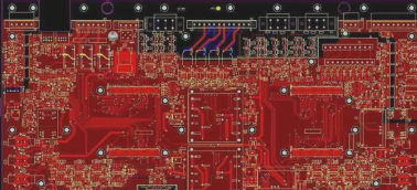
1. The primary goal of micro-etching is to eliminate significant oxides from the copper surface, creating a uniform and bright micro-rough texture. This facilitates finer and more uniform growth of the subsequent OSP film. Typically, the gloss and coloration of the copper surface after OSP film application correlate positively with the chosen micro-etching chemicals, as different chemicals yield varying surface roughness.
2. **Acid Rinse:**
The pickling process thoroughly removes residual materials from the copper surface after micro-etching, ensuring a clean substrate.
3. **OSP Coating (Organic Solderability Preservation Treatment):**
An organic copper complex compound is deposited onto the copper surface to protect it from oxidation during storage. The OSP film thickness is generally required to be between 0.2 and 0.5 micrometers.
4. Factors influencing OSP film formation include:
▪ The pH level of the OSP bath solution
▪ Concentration of the OSP bath
▪ Total acidity of the OSP bath
▪ Operating temperature
▪ Reaction time
5. Post-OSP washing should strictly maintain a pH above 2.1 to avoid excessive acid that could erode the OSP film, compromising its thickness.
6. **Drying:**
To ensure the coating layer on the board surface and in the holes is adequately dried, it is advisable to use hot air at temperatures between 60 and 90°C for 30 seconds. (Note that specific requirements may vary depending on the OSP materials used.)
7. **Advantages of OSP (Organic Solderability Preservative) Surface Treatment on Circuit Boards:**
▪ Cost-effective.
▪ Excellent soldering strength. OSP-treated copper generally exhibits superior soldering strength compared to ENIG nickel treatments.
▪ Expired boards (three to six months) can often be resurfaced, typically allowing for one reapplication depending on their condition.
8. **Disadvantages of OSP (Organic Solderability Preservative) Surface Treatment on Circuit Boards:**
▪ OSP is a transparent film, making thickness measurement and control challenging. Insufficient thickness fails to protect the copper surface adequately, while excessive thickness may hinder solderability.
▪ It is recommended to operate in a nitrogen-rich environment during secondary reflow to achieve optimal soldering results.
▪ Limited shelf life. Generally, the shelf life of OSP-treated boards is up to six months, with some lasting only three months. This depends on the board manufacturer’s capabilities and quality. Boards that exceed their shelf life can often have the old OSP removed and a new layer reapplied, though this process may involve corrosive chemicals that can damage the copper surface. Smaller solder pads may complicate this process, so it’s important to consult with the manufacturer regarding the possibility of re-treating the surface.
▪ Vulnerability to acids and humidity. During secondary reflow soldering, the process must be completed within a specific timeframe. Typically, it is advisable to use OSP-treated boards within 24 hours of opening the package. Ideally, the time between the first and second reflow should be minimized, with recommendations suggesting completion within 8 to 12 hours.
▪ As OSP forms an insulating layer, test points on the board must be printed with solder paste to strip the OSP layer for electrical testing. Related reading: What is ICT (In-Circuit Test)? What are its advantages and disadvantages?
▪ OSP boards are copper-based. Initially, the beneficial IMC of Cu6Sn5 forms after soldering; however, over time, it can degrade to the less desirable IMC of Cu3Sn, which may affect reliability. Long-term reliability considerations for OSP are critical for products with extended service lives.
9. **Perspectives on OSP Surface Treatment for Circuit Boards:**
Given OSP’s low cost and good initial weldability, it is particularly well-suited for mass-produced consumer products. However, the transition of the IMC from beneficial Cu6Sn5 to less favorable Cu3Sn over time should be noted, especially after the warranty period.
10. OSP is not ideal for low-volume, diverse products or those with uncertain demand forecasts. If inventory levels in the circuit board company often exceed six months, using OSP is not advisable.
—
Let me know if you need any further adjustments!

