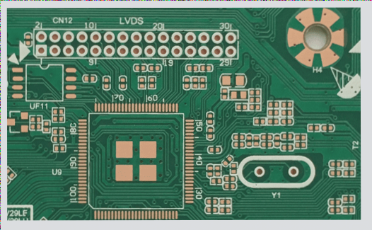
Automated Optical Inspection (AOI) in PCB Manufacturing
Automated Optical Inspection (AOI) is a crucial process in printed circuit board (PCB) manufacturing. It utilizes cameras to autonomously inspect the device under test for critical failures like missing components and quality defects.
Importance of AOI in PCB Manufacturing
- Line width violations
- Spacing violations
- Excess copper
- Missing pads
- Short circuits
- High-frequency applications
- High power load circuits
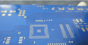
Advantages of AOI Testing
AOI testing employs advanced visual inspection methods to detect surface defects such as opens, shorts, and incorrect or missing components.
Key Advantages of AOI Testing
- Multiple Inspection Objects: AOI is highly effective for inspecting both PCBs and PCB assemblies. It can detect issues like shorts, opens, insufficient solder, component soldering, polarity, and values.
- Cost-Effective: AOI is a more affordable method compared to Automatic X-ray Inspection (AXI) for inspecting solder joint defects.
- High Flexibility: AOI can be implemented at different manufacturing stages based on needs and cost tolerances. It is ideal to perform AOI after reflow soldering to optimize inspection efficiency and reduce costs. Immediate adjustments can be made to manufacturing parameters upon problem identification, ensuring high-quality subsequent products.
If you have any inquiries regarding PCBs or PCBA, do not hesitate to reach out to us at info@wellcircuits.com.