A Ball Grid Array (BGA) is a type of surface-mount package used for integrated circuits. BGAs are typically used to permanently mount devices such as microprocessors. Unlike dual in-line or flat packages, BGAs offer more interconnection pins, each pin being equipped with a solder ball. The connections are evenly distributed in a uniform surface grid or matrix across the component, utilizing the entire bottom surface rather than just the perimeter.
The leads of a BGA are generally shorter compared to those of a perimeter-only package, which enhances performance at high speeds.
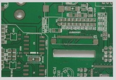
Soldering BGA devices requires precise control and is usually done through automated processes. Due to their design, BGAs are not suitable for socket mounting.
Advantages of BGA:
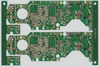
- Efficient PCB Space Utilization: BGA packages reduce the number of components and provide a smaller footprint. This allows for more compact and customized PCB designs, effectively maximizing PCB space usage.
- Improved Thermal and Electrical Performance: The small size of the PCB in BGA packages facilitates better heat dissipation. When the silicon wafer is mounted on top, the majority of the heat can be transferred downward to the ball grid. Conversely, mounting the silicon wafer on the bottom connects the backside of the wafer to the top of the package, which is considered one of the best methods for heat dissipation. Additionally, the lack of pins that can bend or break contributes to stable and reliable electrical performance.
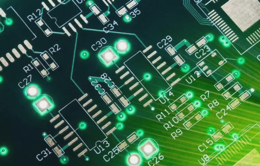
- Increased Manufacturing Efficiency: BGA pads are generally large, which simplifies the soldering process. This results in faster PCB manufacturing and improved yield rates. Larger pads also make rework easier, if necessary.
- Reduced Damage: BGA leads are made of solid solder balls that are less likely to be damaged during operation, enhancing the overall durability of the device.
- Cost Reduction: The combined benefits of space efficiency, enhanced thermoelectric performance, and reduced damage contribute to lower manufacturing costs. The more effective use of PCB space reduces material costs, while better thermal management helps ensure the quality of electronic components, reducing defects.
Wellcircuits BGA Technology:
At Wellcircuits, our typical BGA technology features a minimum size of 0.3mm, with a minimum spacing of 0.2mm between the circuit lines and between two BGA packages. If you have higher requirements, please specify them in your request.


If you have any questions about PCB or PCBA, please contact us at info@wellcircuits.com.