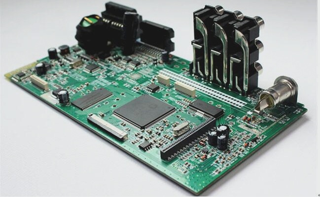
**Introduction to Impedance-Controlled PCB Boards**
An impedance-controlled PCB (Printed Circuit Board) is a type of board designed to manage the impedance of signal traces. Impedance control refers to regulating the “resistance” encountered by high-frequency signals as they travel through a specific layer of the circuit and interact with its reference layer. This resistance must remain within a predetermined range to ensure the signal is transmitted without distortion or degradation. In essence, impedance control ensures that the impedance across different parts of the PCB remains consistent, enabling proper impedance matching. This matching is crucial for maintaining signal integrity, particularly in high-speed and high-frequency applications, where signal reflection and loss can occur if impedance mismatches are present.

**Impedance in PCB Design: Key Considerations and Challenges**
1. **Material Selection and Production Process**
In the production of printed circuit boards (PCBs), several critical processes, such as copper sinking, electroplating with tin, and connector soldering, must be carefully managed to ensure high-quality performance. The materials used during these stages should have low resistivity to maintain the overall impedance of the circuit board at a desired level. A low impedance is essential for meeting product quality standards and ensuring the PCB operates normally within the circuit.
2. **Challenges with Tin Plating**
Tin plating is one of the most critical and problematic steps in PCB manufacturing, as it directly influences impedance performance. The main issues associated with tin plating include discoloration, oxidation, and deliquescence, all of which can compromise the quality of the solder joint. These problems can make soldering difficult, leading to high impedance, poor electrical conductivity, and potentially unstable board performance. Therefore, careful control and quality checks during the tin plating process are essential to maintain low impedance and reliable performance.
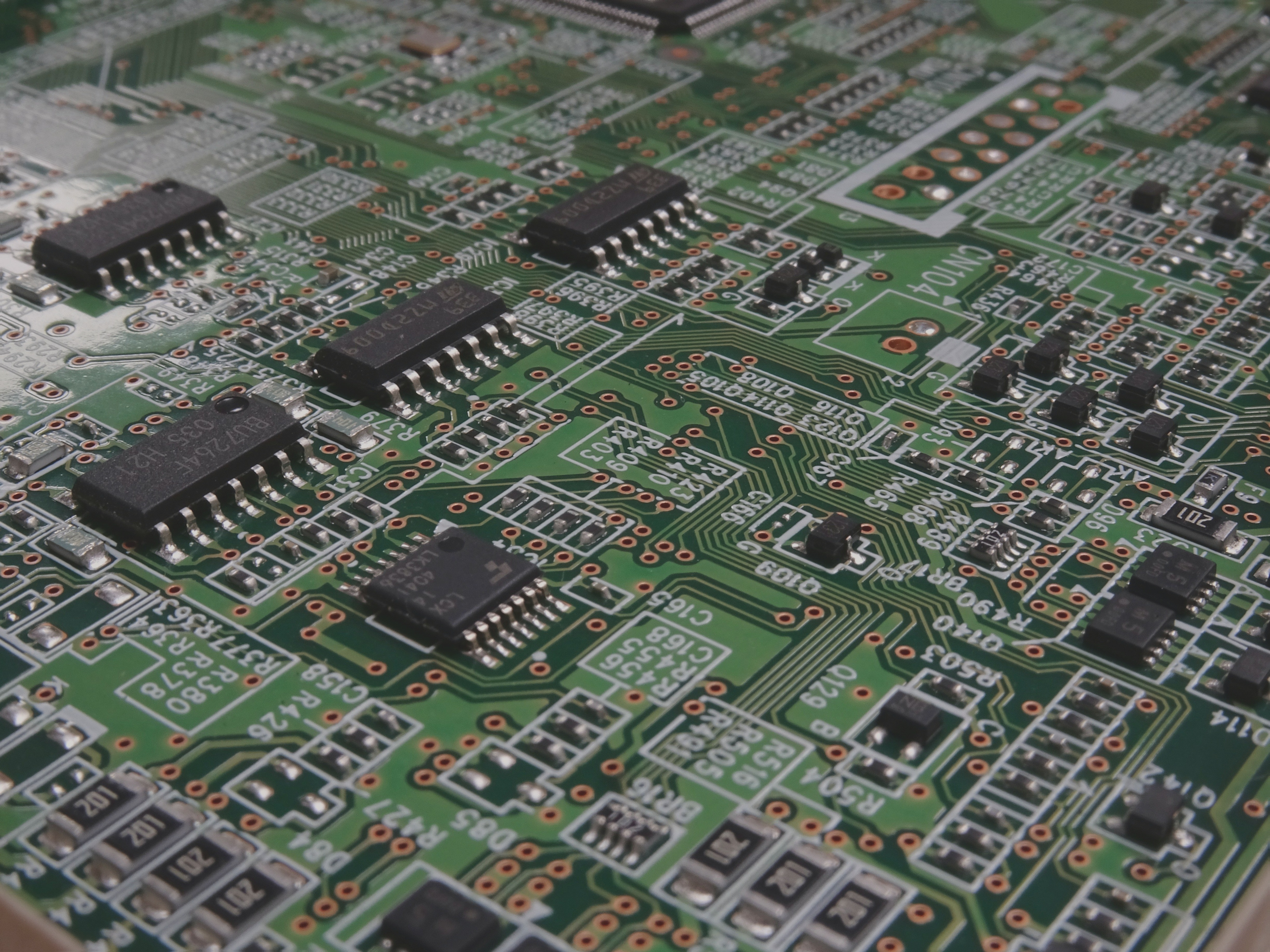
3. **Impact of Frequency on Impedance**
As signal transmission in a PCB involves high-frequency signals, the design must account for the changes in impedance due to various factors such as etching, laminate thickness, and trace width. As the frequency increases to boost transmission rates, the PCB’s impedance can shift, distorting the signal. This can degrade circuit performance. Therefore, it is crucial to control impedance within specific limits to minimize signal distortion and maintain optimal signal integrity.
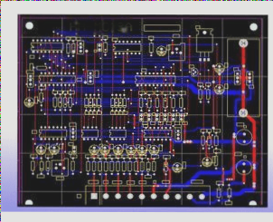
4. **Consideration of Component Placement**
During the PCB design process, careful attention must be paid to the placement of components. Once components are mounted, the overall electrical performance and signal transmission become paramount. In general, a lower impedance is preferred for better signal quality and performance. In particular, minimizing impedance mismatches can help ensure stable and reliable circuit behavior.
5. **False Copper Exposure in PCB Manufacturing**
After the PCB’s copper traces are etched, a layer of ink (often referred to as solder mask or green oil) is applied to protect the copper and prevent short circuits. This ink has fluid properties, and during the curing process, it may sometimes result in uneven application. In some cases, areas of the copper may be exposed, especially if the ink fails to cover certain sections properly. This phenomenon, referred to as false copper exposure, can be detected using a magnifying glass and may lead to issues such as incomplete protection and potential short circuits. Ensuring uniform ink application during the curing stage is critical to avoid this problem and maintain the integrity of the PCB.
In summary, achieving optimal impedance in PCB manufacturing requires meticulous control over material selection, manufacturing processes, and design considerations. By addressing common challenges such as tin plating issues, frequency-induced impedance variations, and potential defects like false copper exposure, manufacturers can ensure that the PCB performs reliably in high-speed, high-frequency applications.
### Reasons for False Copper Exposure in PCB Manufacturing
False copper exposure is a common issue in the PCB (Printed Circuit Board) manufacturing process, often resulting from various factors in the production stages. Below are the main causes, along with recommendations for addressing them:
1. **Improper Solder Mask Process:**
In the solder mask application, during the board cleaning process, the hole plugging network is sometimes not used. Instead, the empty network is used, leading to continuous printing and plugging over unfilled holes. As a result, the plug hole may not be fully filled, and the ink shrinks during the post-baking process, exposing copper along the edges of the hole. This phenomenon, referred to as false copper exposure, can be avoided by ensuring proper hole plugging procedures and quality control during the solder mask curing process.
2. **Ink Residue in Heavy-Duty Board Holes:**
In some cases, ink left inside the holes of heavy-duty boards may not be adequately cleaned. This ink residue prevents proper hole filling during the second printing stage, causing incomplete plug hole filling. The resulting false copper exposure is due to the insufficient plug coverage. To prevent this, it is essential to thoroughly clean the holes before reapplying the solder mask, ensuring that the plug hole is fully filled.
3. **Improper Hole Plugging Due to Flat Printing Table:**
When printing plug holes, the first side of the board is placed directly on the flat printing press table. The flat surface can impede air flow from the holes, causing incomplete plugging in some instances. If the plug hole is not properly filled, it leads to false copper exposure. To solve this issue, the printing setup should be adjusted to allow better air circulation around the holes, ensuring that the plugging process is fully completed.
4. **Lack of Personnel Inspection:**
Inadequate inspection by personnel can lead to missed issues, including false copper exposure. The absence of thorough checks at critical stages of production can result in defective boards being passed through the process. Regular and rigorous inspection procedures must be enforced to identify potential issues before they lead to false copper exposure.
### Recommendations for Addressing False Copper Exposure
When false copper exposure is detected, it’s critical not to proceed with the board’s use, as the impact extends beyond just the board itself. The true cost of the issue is the potential damage to components on the circuit board. Therefore, boards with visible copper leakage should be sent directly back to the original factory for rework or remanufacturing. This ensures that no defective boards make it into the final product, reducing risks and preventing costly losses. Additionally, implementing better quality control processes and improving staff training can significantly reduce the occurrence of false copper exposure.
An impedance-controlled PCB (Printed Circuit Board) is a type of board designed to manage the impedance of signal traces. Impedance control refers to regulating the “resistance” encountered by high-frequency signals as they travel through a specific layer of the circuit and interact with its reference layer. This resistance must remain within a predetermined range to ensure the signal is transmitted without distortion or degradation. In essence, impedance control ensures that the impedance across different parts of the PCB remains consistent, enabling proper impedance matching. This matching is crucial for maintaining signal integrity, particularly in high-speed and high-frequency applications, where signal reflection and loss can occur if impedance mismatches are present.
**Impedance in PCB Design: Key Considerations and Challenges**
1. **Material Selection and Production Process**
In the production of printed circuit boards (PCBs), several critical processes, such as copper sinking, electroplating with tin, and connector soldering, must be carefully managed to ensure high-quality performance. The materials used during these stages should have low resistivity to maintain the overall impedance of the circuit board at a desired level. A low impedance is essential for meeting product quality standards and ensuring the PCB operates normally within the circuit.
2. **Challenges with Tin Plating**
Tin plating is one of the most critical and problematic steps in PCB manufacturing, as it directly influences impedance performance. The main issues associated with tin plating include discoloration, oxidation, and deliquescence, all of which can compromise the quality of the solder joint. These problems can make soldering difficult, leading to high impedance, poor electrical conductivity, and potentially unstable board performance. Therefore, careful control and quality checks during the tin plating process are essential to maintain low impedance and reliable performance.
3. **Impact of Frequency on Impedance**
As signal transmission in a PCB involves high-frequency signals, the design must account for the changes in impedance due to various factors such as etching, laminate thickness, and trace width. As the frequency increases to boost transmission rates, the PCB’s impedance can shift, distorting the signal. This can degrade circuit performance. Therefore, it is crucial to control impedance within specific limits to minimize signal distortion and maintain optimal signal integrity.
4. **Consideration of Component Placement**
During the PCB design process, careful attention must be paid to the placement of components. Once components are mounted, the overall electrical performance and signal transmission become paramount. In general, a lower impedance is preferred for better signal quality and performance. In particular, minimizing impedance mismatches can help ensure stable and reliable circuit behavior.
5. **False Copper Exposure in PCB Manufacturing**
After the PCB’s copper traces are etched, a layer of ink (often referred to as solder mask or green oil) is applied to protect the copper and prevent short circuits. This ink has fluid properties, and during the curing process, it may sometimes result in uneven application. In some cases, areas of the copper may be exposed, especially if the ink fails to cover certain sections properly. This phenomenon, referred to as false copper exposure, can be detected using a magnifying glass and may lead to issues such as incomplete protection and potential short circuits. Ensuring uniform ink application during the curing stage is critical to avoid this problem and maintain the integrity of the PCB.
In summary, achieving optimal impedance in PCB manufacturing requires meticulous control over material selection, manufacturing processes, and design considerations. By addressing common challenges such as tin plating issues, frequency-induced impedance variations, and potential defects like false copper exposure, manufacturers can ensure that the PCB performs reliably in high-speed, high-frequency applications.
### Reasons for False Copper Exposure in PCB Manufacturing
False copper exposure is a common issue in the PCB (Printed Circuit Board) manufacturing process, often resulting from various factors in the production stages. Below are the main causes, along with recommendations for addressing them:
1. **Improper Solder Mask Process:**
In the solder mask application, during the board cleaning process, the hole plugging network is sometimes not used. Instead, the empty network is used, leading to continuous printing and plugging over unfilled holes. As a result, the plug hole may not be fully filled, and the ink shrinks during the post-baking process, exposing copper along the edges of the hole. This phenomenon, referred to as false copper exposure, can be avoided by ensuring proper hole plugging procedures and quality control during the solder mask curing process.
2. **Ink Residue in Heavy-Duty Board Holes:**
In some cases, ink left inside the holes of heavy-duty boards may not be adequately cleaned. This ink residue prevents proper hole filling during the second printing stage, causing incomplete plug hole filling. The resulting false copper exposure is due to the insufficient plug coverage. To prevent this, it is essential to thoroughly clean the holes before reapplying the solder mask, ensuring that the plug hole is fully filled.
3. **Improper Hole Plugging Due to Flat Printing Table:**
When printing plug holes, the first side of the board is placed directly on the flat printing press table. The flat surface can impede air flow from the holes, causing incomplete plugging in some instances. If the plug hole is not properly filled, it leads to false copper exposure. To solve this issue, the printing setup should be adjusted to allow better air circulation around the holes, ensuring that the plugging process is fully completed.
4. **Lack of Personnel Inspection:**
Inadequate inspection by personnel can lead to missed issues, including false copper exposure. The absence of thorough checks at critical stages of production can result in defective boards being passed through the process. Regular and rigorous inspection procedures must be enforced to identify potential issues before they lead to false copper exposure.
### Recommendations for Addressing False Copper Exposure
When false copper exposure is detected, it’s critical not to proceed with the board’s use, as the impact extends beyond just the board itself. The true cost of the issue is the potential damage to components on the circuit board. Therefore, boards with visible copper leakage should be sent directly back to the original factory for rework or remanufacturing. This ensures that no defective boards make it into the final product, reducing risks and preventing costly losses. Additionally, implementing better quality control processes and improving staff training can significantly reduce the occurrence of false copper exposure.