In-Circuit Testing (ICT) for PCBs: Ensuring Proper Functionality
In-Circuit Testing (ICT) is a vital method for testing electronic components and connections on a printed circuit board (PCB) to guarantee their proper functionality. Early implementation of ICT in the manufacturing process helps in identifying and rectifying potential issues before defective products reach customers.

Key Aspects of ICT Testing:
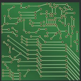
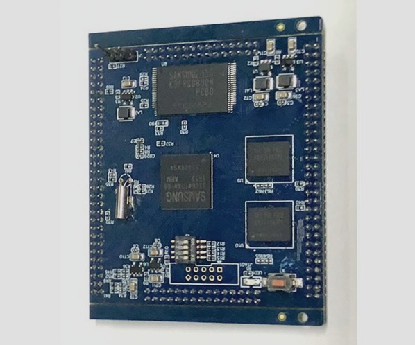
- ICT involves connecting the PCB to specialized testing equipment using test probes to measure parameters like resistance, capacitance, and inductance.
- It checks for correct installation and connection of electronic components, detecting manufacturing defects and assembly errors.
- ICT testing limitations include the inability to detect internal component failures or assess component performance.
ICT testing is usually followed by additional testing methods like functional or system testing to ensure the overall integrity and reliability of the PCB.
Benefits of ICT Testing:
- Speed, reliability, and precision in identifying manufacturing defects and assembly errors early in the production process.
- Complements other testing methods to ensure the integrity and reliability of PCBs in modern electronics manufacturing.
Defects Identified by ICT:
- Software defects: syntax errors, logical flaws, and runtime failures.
- Hardware defects: faulty circuit boards, malfunctioning sensors, or defective connectors.
- Network issues: slow connectivity, DNS errors, and routing complications.
- Security vulnerabilities: insecure protocols, weak passwords, and outdated software.
Advantages of ICT Testing:
- Improved software quality by identifying defects early in the development cycle.
- Reduced development costs by catching defects early and lowering bug-fixing expenses.
- Faster time-to-market by quickly resolving issues and accelerating the development process.
- Increased customer satisfaction through high-quality, defect-free software products.
- Competitive advantage by delivering reliable software products faster than competitors.
- Enhanced security by detecting vulnerabilities before they can be exploited.
Disadvantages of ICT Testing:
Drawbacks of ICT Testing in Organizations
- High Initial Investment: Implementing an ICT testing program can be expensive due to the need for specialized equipment and skilled personnel. Additionally, resolving defects found during testing can escalate costs.
- False Security: ICT testing can uncover various defects but cannot ensure bug-free software. Depending solely on ICT testing may create a false sense of security if other tests or security evaluations are overlooked.
- Limited Detection: ICT testing may miss certain defects like user experience issues or compatibility problems with specific hardware or software setups. Moreover, it might not be suitable for specialized software such as embedded systems.
- Time-Intensive: Conducting ICT testing, especially for large or intricate software, can be time-consuming and lead to delays if not adequately planned.
- Tool Dependency: ICT testing often relies on costly specialized tools that demand extensive training for effective usage. Excessive reliance on these tools can hinder the transition to alternative testing methods.
To maximize the benefits of ICT testing, organizations must acknowledge these drawbacks and formulate a comprehensive testing approach that addresses these challenges.
If you have any inquiries regarding PCBs or PCBA, please don’t hesitate to reach out to me at info@wellcircuits.com