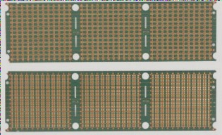
The printed circuit board (PCB) assembly process comprises several processes and rules that must be followed in the correct order for the end product to function correctly. PCB producers employ screen templates and regulated heating and cooling processes to govern how components are placed and fixed into place to ensure this happens.
When assembling a printed circuit board, you must select the appropriate technology for the components.
All parts and pieces must be aligned correctly in their appropriate locations, as stated in the PCB design. No matter how minor, any divergence might have a significant impact on the finished board’s functionality.
Step By Step Process Of PCB Assembly
We have the process easier for you by dividing the whole process of PCB Assembly into simple, digestible steps given below.
Apply Solder Paste By Using Stencil
The first step in the PCB Assembly procedure is applying solder paste to the printed circuit board. You can think of this process as screen printing a shirt, but the only difference is that the assembly process involves the usage of thin steel, which is stainless as well called a stencil, instead of a mask.
The addition of stencil allows you to apply solder paste to certain specified parts of the PCB to attach components.
The solder paste itself is nothing complex but a grayish paste composed of tiny metal balls. These metallic balls are about 96% tin and 03% silver, and the remaining 0.5% is copper. Accordingly, the solder paste helps in the mixing of solder and flux. You should know that the flux is a chemical specifically designed to help melt the solder and thus enable it to stick to the required surfaces.
A mechanical fixture keeps the PCB and solder stencil in place on a professional PCBA line. An applicator then precisely applies solder paste to the desired regions. The paste is then evenly applied to every open region of the stencil by the machine. The solder paste remains in the intended spots once the stencil is removed.
Pick And Place Of Components
Following solder paste application to the PCB board, the PCBA process proceeds to the pick and place machine, where a robotic device installs surface mount components, or SMDs, on a prepared PCB. SMDs now account for the majority of non-connector components on PCBs. In the following phase of the PCBA process, these SMDs are soldered to the board’s surface.
Traditionally, this manual operation required assemblers to pick and place components by hand using a pair of tweezers. This procedure is now, thankfully, an automated process among PCB producers. This transition mainly happened because machines are more accurate and consistent than humans. While humans can work swiftly, tiredness and eye strain are common after a few hours of working with such small components. Machines can work around the clock without becoming tired.
The gadget begins the pick and place process by vacuum gripping a PCB board and transporting it to the pick and place station. The robot subsequently positions the PCB at the station and starts adding SMTs to the PCB surface. These components are positioned in predetermined locations on top of the soldering paste.
Reflow Soldering Step
Reflow soldering is the third stage after the components have been set and solder paste has been applied. The reflow soldering procedure involves placing the PCBs and components on a conveyor belt. This conveyer belt subsequently transports the PCBs and components into a large oven, heated to 250o C. This temperature causes the solder to melt. Melted solder will then adhere the components to the PCB and form joints.
After being subjected to high temperatures, the PCB is placed in cooling. The solder junctions are subsequently solidified in a regulated manner by these coolers. This will form a permanent connection between the SMT component and the PCB. In the event of two-sided PCBs, the PCB side with fewer or smaller components will be treated first from steps 1 to 3, followed by the other side.
Quality Control And Inspection
After the surface mount components are soldered during the reflow process, the PCBA is incomplete, and the finished board must be checked for operation. Movement during the reflow process frequently results in poor connection quality or no connection. Shorts are another common side consequence of this movement, as misplaced components can sometimes join circuit segments that should not be connected. Several inspection procedures can be used to check for these faults and misalignments. The following are the most popular examination methods.

Manual Examination:
Because the PCB contains microscopic SMT components, visually inspecting the board for misalignment or flaws can cause tiredness and eye strain for technicians. As a result of the incorrect findings, this approach is unsuitable for advanced SMT boards. This strategy, however, is practical for boards with THT components and a lower component density.
Optical examination:
This method is feasible for significant quantities of PCB. This technology uses an automated machine outfitted with high-powered, high-resolution cameras positioned at various angles to view solder connections from multiple angles. Depending on the integrity of the solder joints, the light will reflect them at different angles. This automated Optical Inspection (AOI) equipment is high-speed and can process vast batches of PCBs in a brief time.
X-ray Inspection:
X-rays are used in yet another type of inspection. This is a less common inspection method typically employed on more complex or stacked PCBs. The X-ray allows the observer to see through layers and visualize lower layers to identify any potentially concealed issues.
The PCBA company’s requirements determine a defective board’s fate; it will be returned to be cleared and fixed or discarded.
Whether or not an inspection uncovers one of these errors, the next stage is to test the part to ensure it accomplishes what it’s supposed to do. This includes checking the quality of the PCB connections. Boards that require programming or calibration necessitate additional actions to ensure proper functionality. Such inspections can be performed regularly following the reflow procedure to identify potential concerns. These regular inspections can assist ensure that faults are discovered and corrected as soon as possible, saving both the manufacturer and the designer time, effort, and materials.
Insertion Of Components
Depending on the type of board under PCBA, the board may incorporate components other than SMDs.
Plated through-hole components, or PTH components, are examples of these.
A plated through-hole is a hole in a printed circuit board plated all the way through. PCB components use these holes to transmit signals from one side of the board to the other. Soldering paste will not work in this situation since it will run right through the hole with no chance of adhering. As a result, the two most common methods of THT component soldering or prototype PCB assembly are
Manual Soldering:
Manual soldering is the most widely used methodology and often takes longer than automated SMT setup. Typically, one technician is assigned to insert one component at a time before passing the board to another technician who inserts another component on the same board. As a result, the board will be moved around the manufacturing line as the PTH components are crammed onto it. As a result, many
PCB designs and manufacturing businesses avoid employing PTH components in their circuit design. However, PTH components remain the most popular and widely used components among circuit designers.
Wave Soldering:
Wave soldering is an automated form of manual soldering. Once the PTH components are placed on the PCB, it is placed on the conveyer belt and moved to a specialized oven. A wave of molten solder is splashed over the bottom layer of the PCB, where the component leads are present. This will solder all of the pins at the same time. However, this procedure is only applicable to single-sided PCBs and not double-sided PCBs since the molten solder used while soldering one side of the PCB can harm components on the opposite side. Following that, the PCB is relocated for a final inspection.
After the soldering procedure is completed, the PCB can go to the final inspection or repeat the previous processes if the PCB requires extra parts or another side to be assembled.
Final Examination and Testing after the PCB Assembly Process
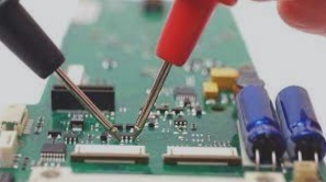
After the soldering phase of the PCBA process is completed, the PCB will be tested for functionality. This is referred to as a “functional test.” The test takes the PCB through its paces, imitating the stable operating conditions of the PCB. In this test, power and simulated signals are passed across the PCB while testers examine its electrical properties.
The PCB fails the test if any of these properties, including voltage, current, or signal output, display unacceptable variation or hit peaks outside a predetermined range. The faulty PCB can then be recycled or trashed depending on the company’s criteria.
Testing is the final and most essential step in the PCB assembly process, as it decides the process’s success or failure. This testing is also critical to performing regular testing and inspection during the assembling process.
What Should You Do After The PCB Process?
Now that the PCB has been tested and certified safe in all respects, it is time to remove the undesired residual flux, finger dirt, and oil stains. All forms of grime can be cleaned with a stainless steel high-pressure washing tool and deionized water. The deionized water will not harm the PCB circuit. After washing, the PCB is dried with compressed air. The final PCB is now ready for packing and shipping.
Conclusion
That was the most accessible guide about the PCB Assembly process and how you can do it yourself. In this summary, the PCB assembly procedure for producing loaded printed circuit boards has been dramatically simplified. The PCB assembly and production procedures are generally tuned to ensure deficient defect levels and, as a result, the highest quality output.


