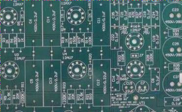
Understanding PCB Back Drilling
PCB back drilling is a crucial process that involves removing via stubs from the inner layers of a multilayer PCB. These via stubs can lead to signal reflections, impacting performance. By eliminating via stubs, back drilling ensures consistent impedance alignment, improving signal integrity, especially in high-speed communication systems and sensitive analog circuits.

How Does Back Drilling Work?
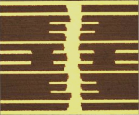
Back drilling employs a CNC machine to remove via stubs from the opposite side of the PCB. The back-drilled hole is slightly larger than the via, preventing damage to surrounding layers while maintaining signal path integrity.
Factors Affecting Back Drilling
- Board Material and Thickness: The type and thickness of the PCB impact back drilling. Different materials may require specific drilling parameters.
- Via Size and Spacing: Vias’ size and spacing determine drilling precision, with smaller vias needing more accurate drilling.
- Trace and Plane Clearance: Adequate clearance between the drill bit and adjacent features is crucial to prevent accidental damage.
For your PCB back drilling needs, you can specify requirements when ordering from Wellcircuits.

If you have inquiries about PCBs or PCBA, contact us at info@wellcircuits.com.