Understanding PCB Design: A Comprehensive Guide
What is PCB?
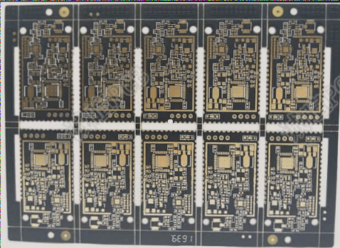
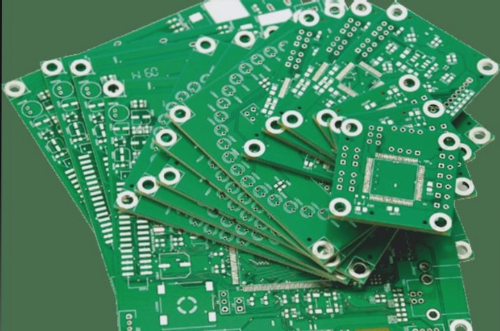
PCB, short for Printed Circuit Board, revolutionized electronic product design by replacing messy point-to-point wiring with a more organized and secure system.
A PCB consists of lines and pads that allow for efficient connections between components, ensuring a reliable model and cost-effectiveness.
Composition of PCB
A PCB may appear as a single layer, but it is actually composed of multiple layers stacked together to form a circuit board.
Silkscreen
The topmost layer on a PCB is the silkscreen, usually white or silver, used for annotations, connection points, and labeling.
Solder Mask
The solder mask, typically green, insulates the copper traces on the board, preventing contact with other metals.
Copper
Copper is laminated above and below the substrate to provide conductivity, with the thickness measured in ounces per square foot.
FR4
FR4, a heat-resistant fiberglass material, serves as the core substrate for PCBs, ensuring durability and reliability in electronic designs.
Basic Steps for PCB Design
Understanding the composition of a PCB is essential before diving into the design process. Here are the fundamental steps involved:
- Conceptualization: Define the basic concept and functionality of the PCB design.
- Schematic Design: Create a schematic layout of the circuit board.
- Component Placement: Position components strategically on the board.
- Routing: Establish connections between components through copper traces.
- Verification: Double-check the design for errors or inconsistencies.
- Production: Once verified, proceed with the fabrication of the PCB.
Mastering PCB design is crucial for ensuring the efficiency and reliability of electronic products. Start your journey into the world of PCB design today!
Understanding the PCB Design Process
1. Initial Considerations
Before diving into PCB design, it’s crucial to determine the intended use of the final product. This helps in planning the wiring points and interconnections with other circuits, taking into account factors like temperature range and environmental considerations.
2. Schematic Design
Once the basic concept is clear, the schematic design phase begins. Sketch out the necessary components, dimensions, and materials required for the PCB design. Keep track of the costs associated with each item for better budget management.
3. Block Diagram
Prior to actual PCB creation, create a block diagram either on paper or digitally. Label the components, wiring, and connection points within designated boxes. This preliminary step streamlines the subsequent PCB design process.
4. Component Placement
After finalizing the block diagram, focus shifts to component placement. Experiment with different positions to optimize functionality, considering that not all placements may work effectively on the first try.
5. Routing
Following component placement, determine the routing of each element on the circuit board to ensure proper connections and functionality.
6. Testing
Conduct thorough testing to validate the connections and functionality of the PCB design. Regular testing helps in identifying and rectifying any issues in component placement and routing.
Few Key Factors for PCB Layout Design
1. Manufacturing Processes
Understanding the specific manufacturing processes required for your PCB design is essential to meet the project’s needs effectively.
2. Board Constraints
Prioritize determining the correct board size based on the final product’s placement and the number of components to be accommodated.
3. Materials and Components
Ensure you have all necessary materials and components ready before commencing the PCB design process to facilitate smooth progress and account for any potential shortages.
4. Placement
Strategic component placement is crucial for effective PCB design, requiring careful consideration of circuit positioning, holes, and connections to minimize errors.
5. Orientation
Arrange similar components in a specific order to streamline the assembly process and reduce confusion during placement.
6. Organization
Prioritize organizing components based on their usage sequence to enhance assembly efficiency and prevent oversight of crucial steps.
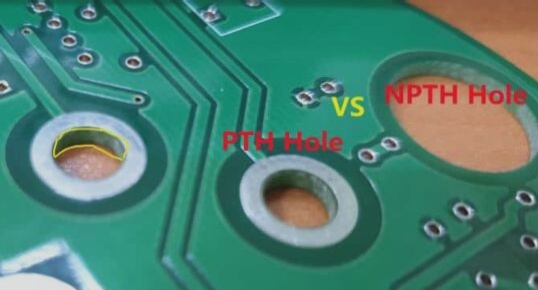
7. Pad and Hole Dimensions
Ensure consistent pad and hole dimensions on the board to facilitate proper alignment of components during assembly.
8. Thermal Check
Conduct a thermal check to verify the materials’ heat resistance, ensuring they can withstand the expected temperatures within the circuit.
Conclusion
Consistent testing throughout the PCB design process is key to ensuring functionality and reliability. PCBs play a vital role in modern electronics, streamlining complex wiring into compact circuit boards. By following these guidelines, you can create your PCB design efficiently while avoiding common pitfalls.