Today I will give you a brief introduction: PCB Gold Finger .
1. What is PCB gold finger?
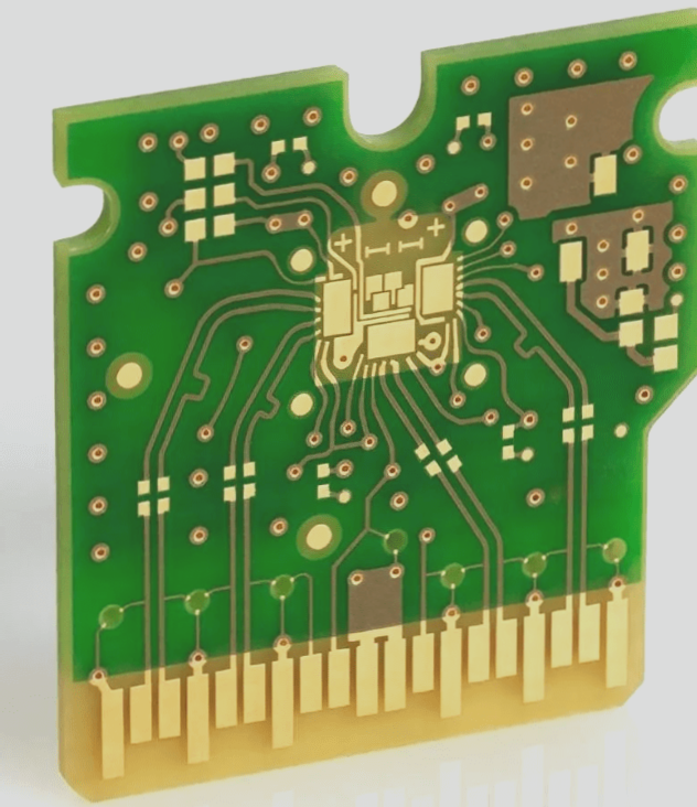
PCB gold fingers are gold-plated posts seen on the edges of PCB connections . The purpose of the gold finger is to connect the auxiliary PCB to the computer’s motherboard. PCB gold fingers are also used in a variety of other devices that communicate via digital signals, such as consumer smartphones and smart watches. Gold is used for connection points along the PCB due to the alloy’s excellent electrical conductivity.
PCB gold fingers can be divided into three types:
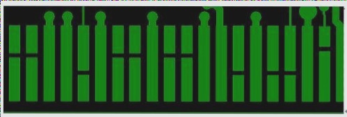
- Ordinary PCB gold fingers – The most common PCB gold fingers, with levels or even arrays . PCB pads have the same length, width, and spacing.

- Uneven PCB gold fingers – PCB pads have the same width but different lengths and sometimes different spaces .
For some PCBs, the gold fingers are designed to be shorter than others. The most relevant example of this type of PCB is a PCB for a memory card reader, where the device connected to the long finger must first power the device connected to the shorter finger.
- Segmented PCB gold fingers – PCB pads come in different lengths and the gold fingers are segmented . The segmented gold fingers vary in length, and some of them are disjointed within the same finger on the same PCB. This PCB is suitable for waterproof and rugged electronic products.

2. PCB Gold Finger Gold Plating Detailed Tutorial
1. Electroless nickel immersion gold (ENIG)
This gold is more cost effective and easier to solder than electroplated gold , but its soft, thin (typically 2-5u” composition makes ENIG unsuitable for the abrasive effects of circuit board insertion and removal .
2. Electroplating hard gold
This gold is solid (hard) and thick (usually 30u”) , so is better suited to the abrasive effects of continuous use on PCBs .
Goldfinger enables different circuit boards to communicate with each other. From the power source to the device or device, a signal must pass between multiple contacts in order to execute a given command.

When a command is pressed, the signal is passed between one or more circuit boards and then read. For example, if you press a remote command on your mobile device, a signal is sent from the PCB-enabled device in your hand to a nearby or distant machine, which in turn receives the signal through its own circuit board.
3. What is the PCB gold finger plating process?
Here is an example, the process of hard gold plating to PCB gold finger is:
1) Cover with blue glue
Except for the PCB gold finger pads that need to be plated with hard gold, the rest of the PCB surface is covered with blue glue. And we align the conductive locations with the direction of the board.
2) Remove the oxide layer on the copper surface of the PCB pad
We use sulfuric acid to remove the oxide layer on the PCB pad surface, and then clean the copper surface with water. We then grind to further clean the PCB pad surface. Next, we clean the copper surface using water and deionized water.
3) Nickel plating on copper surface of PCB pad
We electroplated a nickel layer on the surface of the cleaned gold finger pad by applying electricity. Next, we use water and deionized water to clean the nickel-plated pad surface.
4) Electroplating gold on nickel-plated PCB pads
We apply electricity to electroplating a layer of gold on the surface of the nickel-plated PCB pad. We recycle the remaining gold. Then we still clean the surface of the gold finger with water first and then deionized water.
5) Remove the blue glue
Now, the hard gold plating of the PCB gold fingers is completed. We then removed the blue glue and continued PCB fabrication to the solder mask printing step.

An edge connector socket consists of a plastic box that is open on one side and has pins on one or both ends of the longer edge. Typically, connectors contain bumps or notches for polarity to ensure that the correct device type is plugged into the connector. The width of the socket is chosen according to the thickness of the connecting plate. On the other side of the socket is usually an insulation-piercing connector that connects to the ribbon cable. A motherboard or daughter card can also be connected to the other side.
2. Special adapter
Goldfinger can add many performance-enhancing features to a personal computer , allowing the computer to provide enhanced graphics and high-fidelity sound through an auxiliary PCB that plugs vertically into the motherboard. Since these cards are rarely individually connected and reconnected, the gold fingers are often more durable than the cards themselves.
3. External connection
Peripheral devices that have been added to the computer station are connected to the motherboard through PCB gold fingers . Equipment such as speakers, subwoofers, scanners, printers, and monitors all plug into specific slots on the back of the computer tower. In turn, these slots connect to the PCB that connects to the motherboard.
4. PCB golden finger design
1. Plated through holes should be kept away from gold fingers
2. For PCB boards that require frequent plugging and unplugging, the gold fingers generally need to be plated with hard gold to increase the wear resistance of the gold fingers. While electroless nickel immersion gold can be used and is more cost-effective than hard gold, it is less wear-resistant.
3. Gold fingers need to be chamfered, usually 45°, other angles such as 20°, 30°, etc. If there are no chamfers in the design, there is a problem. As shown in the figure below, the arrow indicates a 45° chamfer:
4. The gold finger needs to be soldered and windowed , and the PIN does not need to open a steel mesh.
5. The minimum distance between the immersed tin and immersed silver pads from the fingertip is 14 mils. It is recommended that the distance between the pad and the gold finger should be at least 1mm, including the via pad.
6. Do not apply copper on the surface of the gold finger .
7. All the inner layers of the gold finger need to be copper cut . Generally, the width of copper is 3mm, and half-finger copper and full-finger cutting can be done. In the PCIE design, there are indications that the copper of the gold finger needs to be completely removed.
The impedance of the gold finger is low, and copper cutting (under the finger) can reduce the impedance difference between the gold finger and the impedance line, which is also good for ESD.
Disclaimer: This article is reproduced from the Internet , and the copyright belongs to the original author. If there are any copyright issues related to the work, please contact us in time, thank you!
Join the fan communication group
Zhang Fei Jianzhan Electronics has opened an exclusive learning and exchange group for fans of the public account. Students who want to join the group for learning and discussion/receiving documents can scan the operation QR code in the picture to join with one click~


