Guide to PCB Encapsulation and Component Packaging
Introduction to PCB Encapsulation
PCB Encapsulation is crucial for establishing the interface between electronic components and the PCB, providing vital information for assembly and maintenance.
Types of Component Packaging
- SOP (Small Outline Package): Compact IC packaging, typically 0.4″ x 0.4″.
- QFP (Quad Flat Package): Larger IC footprint, ranging from 0.8″ x 0.8″ to 1″ x 1″.
- BGA (Ball Grid Array): Large IC package with multiple connections, from 0.5″ x 0.5″ to over 2″ x 2″.
Essential Elements of PCB Encapsulation
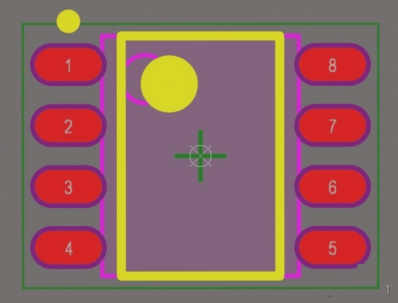
- Pads / Holes: Critical for precise soldering and component placement.
- Component Outline: Defines the area for component placement.
- Reference Indicator: Unique codes for component identification.
- Pin 1 Indication: Clear marking of pin 1 location for assembly clarity.
- Mechanical Information: Considerations for mechanical parts.
- 3D Models and Symbols: Aid in correct component positioning.
Global Standards for PCB Packaging
International standards like IPC 7351 set guidelines for PCB packages, symbols, and 3D models.
Latest Innovations in PCB Encapsulation
Recent advancements focus on improving component integration, precise assembly, and space optimization.
Future Trends in PCB Encapsulation
The future may bring miniaturization, higher component density, and advanced materials for better performance.
Standards and Guidelines for PCB Packaging
- IPC 7351 Standard: Controls component pad sizes for design compliance.
- ANSI Y32.2-1975: Defines graphical symbols for electrical drawings.
- ISO 10303-21: Specifies STEP model file format for 3D CAD software.
Key Design Considerations for PCBs:
- Pad Size: Match pads with component leads for safe connections.
- Pad Spacing: Ensure proper spacing for soldering and electrical connections.
- Pad Shape: Align pad shapes with component leads for secure connections.
- Through-Hole Placement: Accurately place through-holes for secure connections.
- Reference Marks: Place reference markers for component identification.
- Clearance and Creepage Distance: Maintain safe distances to prevent shorts.
- Alignment Width: Ensure alignments support stable current flow.
View an example of a well-designed PCB package below:
For further insights on PCB packaging and design, consult a PCB specialist.