A printed circuit board (PCB) is one of the most important electronic devices that has been used in the modern world. We can’t think of any single electronictech device that doesn’t need a PCB. But before we implement the characteristics of a PCB, we have to undergo some steps to assemble the PCBs. This process is called the assembling of PCBs. There are certain strict steps that a PCB has to go through before getting properly assembled. And one of the major and last steps before the successful assembling of a PCB is the PCBA (Printed circuit board assembly) has to be tested. This step is essential as it ensures that the manufacturers don’t receive the faulted PCBA. Therefore, if you want to know more about PCBA testing, you are at the right place. It is because, in today’s article, we will explore PCBA testing in great depth. Thus, keep reading this article till the end to get the best out of it.
Before we dive into the major details, let’s have a brief overview of the technical meaning of PCBA testing.
What is PCBA testing?
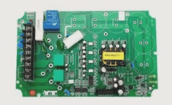
PCBA testing is the process of determining the electrical conductivity of a printed circuit board containing electronic components and detecting it using input and output values. There are numerical relationships between distinct test points in the PCBA item test, such as voltage and current. To check whether the real PCBA board fits the design requirements, professional test equipment or a manually operated multimeter must be used to detect the test points. PCBA testing is an important step in ensuring manufacturing and delivery quality. Any PCBA maker should adhere to PCBA testing standards and conduct tests in accordance with the customer’s test plan.
PCBA testing is based upon one concrete principle. Do you want to know what the PCBA testing principle is? To know about on what basis a PCB is tested, Read on!
What’s the PCBA testing principle?
The FCT (Functional Circuit Test) fixture connects the test points on the PCBA circuit board to make a complete circuit that connects the computer and the programmer and uploads the MCU (Microcontroller Unit) software. The MCU application will catch the user’s input action and apply calculations to turn on and off neighboring circuits or drive motor rotation. To complete the PCBA item test, observe the voltage and current values between the test points on the FCT fixture and verify that these input and output actions are compatible with the design.
So, we have mentioned the FCT fixture (Functional Circuit Test), but what is the PCBA Testing fixture? Let’s have a look at it below!
What’s PCBA Testing Fixture?
Large volumes of PCBA circuit boards must be examined, and a corresponding PCBA test fixture is frequently provided to help with this. To fulfill the goal of speedy PCBA testing, the PCBA test fixture connects the test needles and test points on the PCB board, obtains voltage, current, and other essential data, and then displays it on the test fixture’s display screen. Engineers will analyze their test schemes, reserve PCB test points, and give professional test documentation or test plans to manufacturers when clients are designing PCB boards.
As you must have guessed by now that PCBA testing isn’t simple as it sounds. The technicians have to deal with many complications and complex steps for PCBA testing. The PCBA testing is further divided into different types, depending upon your needs. We will be discussing each type in great depth below.
What are the types of PCBA testing?
There are several ways for PCBA testing, and the manufacturers decide the one that is most beneficial for them. However, we are going to mention the most famous ways for the testing of PCBA that are been used worldwide by international manufacturers. The well-known ways of PCBA testing are as follow:
- Automated Optical testing.
- In-Circuit Testing Method.
- Built-in Self-Test.
- X-Ray Inspection.
You might have heard about the famous Automated Optical Testing if you have a mild idea about the PCB assembly process. And even if you don’t know, you need not worry about it. We will try our best to explain each of these matters comprehensively.

Automated Optical Testing:
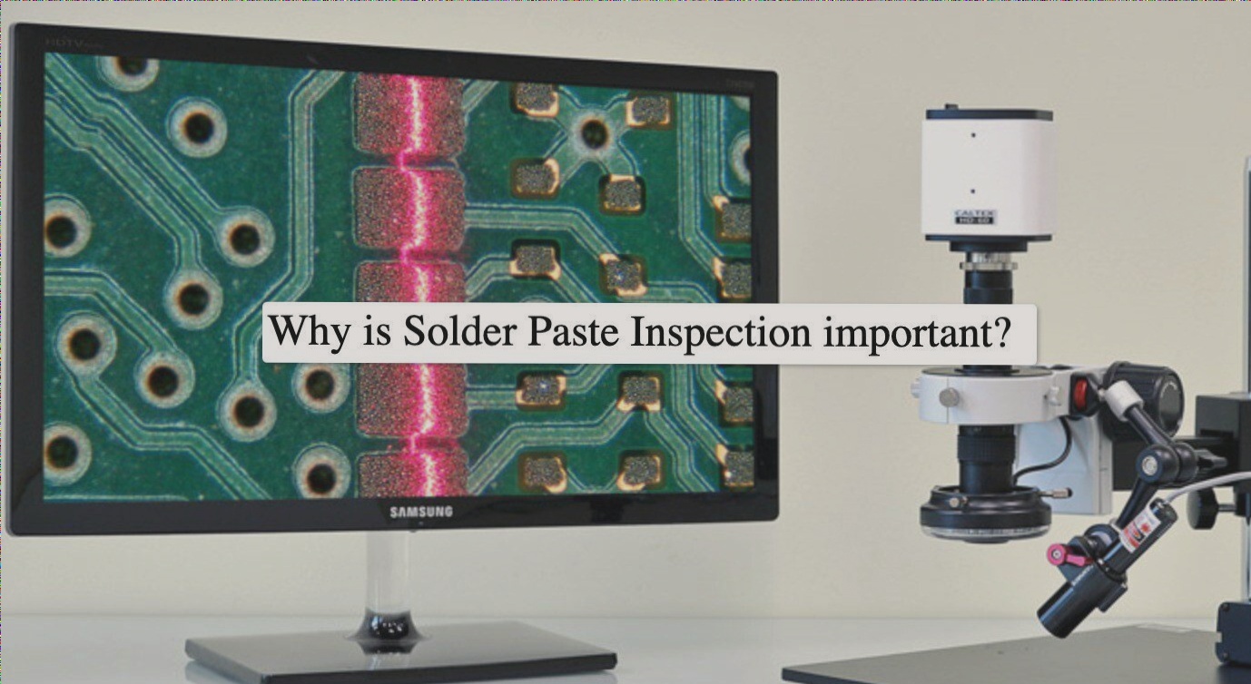
It’s the widely used process for PCBA Testing due to several factors. In the process of PCB assembly, the PCB is tested to check if the PCB has any faults. To use Automated Optical Testing, the PCB is usually tested after reflow soldering in SMT (Surface Mount Technology) assembly. To obtain photos of the PCB assembly, this method employs numerous cameras or microscopes. After that, the photos are compared to reference photographs using the software. This method can also test the end product’s quality and offer a visual record of the PCB assembly process. Automated Optical Testing substitutes human visual inspection with greater precision and speed. Missing components, misplacement, misalignment, overall quality, and PCB assembly measurements are all common problems that can be detected with AOI. As you can easily guess why this process is widely used, it is because of its speed. It is a highly fast process and gives out results in a matter of seconds. Moreover, you can run out this test on any volume of PCB. However, you can only get the test result of the surface of a PCB. That’s why you have to use this test with another type of PCBA testing that gives you the results for the inner structure of PCBA.
In-Circuit Testing Method:
The In-Circuit Testing (ICT) is run on the PCB at the end of the PCB assembly. The ICT is a complex structure that involves the functionalities of multiple machines at the same time. Test probes that connect to test locations on the PCB connect the test system to the PCB. Circuits and components are electrically tested against critical values. It detects manufacturing flaws and verifies PCB functionality against specifications. Solder shorts, missing components, component failures, raised pins, component shifts, and poor soldering difficulties are the most prevalent defects that ICT can detect. The standard bed of nails test and the flying probe test are the two tests available for in-circuit testing.
Standard bed of nails test:
Fixtures are used to connect the assembled PCB to the tester in ICT machines. A fixture is made up of probes (needles) that are connected to specified test spots on the PCB. Fixture wires link the probes to the fixture interface pins. These cables allow you to swap out probes for different PCB test sites. The pins on the fixture link to the pins on the testing module. Through this interface, the tester sends a series of various signals to the PCB and receives signals back. To detect any anomalies, the tester compares the received signals from the PCB to standard signals for the specified PCB. Machines for in-circuit testing exist. As the machine cannot access test spots on new densely packed PCBs, and as PCBs are becoming increasingly complex, this method is becoming less and less popular. Moreover, this method is highly expensive and doesn’t work on modern densely packed boards.
Flying Probe ICT:
Flying probe testing is another ICT system that conducts tests using two or more probes that can move across the PCB board and lower probes on test pads. It runs tests in sequential order. This method can be used to test high-density PCBs, PCBs that don’t fit into normal ICT test rigs, and PCBs with small connections (0.2mm test pitch). In this test, you don’t need the test fixtures. However, this process isn’t fast and takes a lot of time comparatively.
Built-in Self-Test:
This method allows the PCB assembly to self-test. Built-in self-test systems not only provide high-reliability checks during manufacturing, but they can also assist at a later stage, such as when a PCB repair is needed. By decreasing the test cycle duration and having a complicated setup of In-circuit testing (testing with probes) approaches, BIST systems make PCB assembly testing simpler. This method is implemented at the last stage of PCB assembly. And this process is highly reliable and even helps the manufacturers with the repairing process.
X-Ray inspection:
The X-Ray inspection is used for discovering faults that are not visible using Automated Optical Inspection. AXI is used to verify solder connections beneath ball grid array (BGA) packages with solder joints underneath the chip packaging. In the manufacturing process, X-ray inspection is usually done on a sample basis. This procedure is often used to check for internal faults in silicon wafers. AXI is accessible in two formats: 2D and 3D. This procedure is often regarded as an extremely expensive PCB assembly testing method. As this technique involves X-Ray, it gives you the highest level of precession in the test, but still, it requires a high machine cost.
Final thoughts:
From the above-given facts, we have discussed all the necessary information that you need to know about PCBA Testing. We have discussed all the widely-known Testing methods in our article, and we tried to make it as simple as we could so that you can easily comprehend each of these ways even if you are studying it for research purposes.
If you have any questions regarding the PCBA Testing, let us know in the comment section below!


