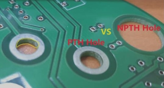
Understanding PTH (Plated Through Hole) in PCBs
PTH, or Plated Through Hole, is a crucial element in circuit board design. These holes are conductive, connected to copper layers, enabling electrical connectivity. On the other hand, NPTH (Non-Plated Through Hole) does not have copper plating, serving as electrical isolators.
Applications of PTH in PCBs
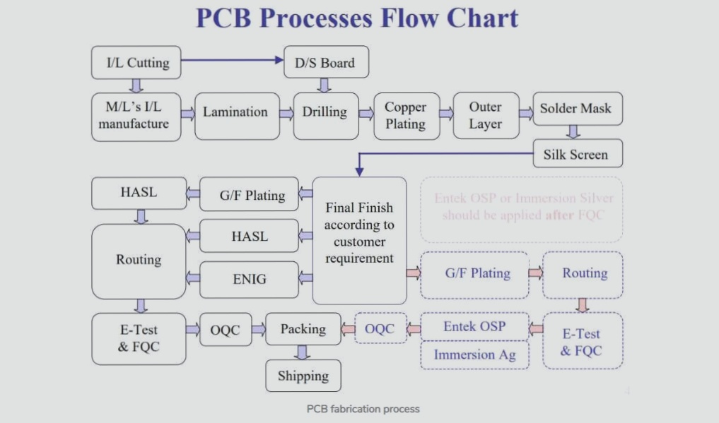
PTH holes serve two main purposes in circuit boards. They are used for soldering traditional DIP component pins, where the hole diameter needs to be slightly larger than the pin diameter for proper insertion. Additionally, smaller PTHs, known as vias, are used to connect copper conductor lines between layers in multi-layered PCBs.
Enhancing PCB Stability
After drilling, a thin copper layer is applied to the walls of PTH holes, ensuring lower connection resistance between component leads and copper traces. This process enhances mechanical stability after PCB assembly.
Advanced PTH Processes
Modern PCB fabrication involves a series of steps for PTH, including alkaline degreasing, micro etching, pre-activation, activation, desmear, and copper deposition. Each step plays a crucial role in ensuring the quality and effectiveness of the PTH process.
Importance of Copper Deposition
Through-hole plating, or chemical copper plating, deposits a thin layer of chemical copper onto non-conductive hole walls, laying the foundation for subsequent copper plating operations. This process is essential for achieving high-quality results in PCB manufacturing.