PCB Reverse Engineering: Key Steps and Considerations
Understanding the Importance of Reverse Schematic Diagrams
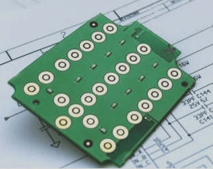
When it comes to PCB reverse engineering, the reverse schematic diagram plays a crucial role in illustrating the working principle and operational conditions of a PCB. Whether derived from PCB files or physical product descriptions, the circuit diagram serves as a tool to analyze functional characteristics.
Essential Steps in Reverse Engineering a PCB Schematic
-
Reasonable Division of Functional Areas
Efficient reverse engineering starts with a well-structured division of functional areas on the PCB schematic. By identifying core components and grouping related elements, engineers can streamline the drafting process.
-
Select Appropriate Reference Components
Choosing key reference components is crucial for building an accurate network map. Engineers typically opt for prominent circuit elements like integrated circuits or transformers for this purpose.
-
Correctly Distinguish and Route the Wires
Understanding power supply design and circuit connections is essential for wire differentiation. By analyzing component connections and using distinct colors for wires, engineers can enhance clarity in the schematic.
-
Master the Basic Framework and Learn from Similar Schematics
Engineers should grasp electronic circuit design principles and study existing schematics to improve efficiency. Recognizing commonalities in schematic layouts among similar products can also aid in the design process.
-
Optimize and Validate the Schematic
After adjusting and optimizing the schematic, thorough testing and inspection are necessary to ensure its accuracy. Validation is the final step in completing the reverse engineering process.
By following these key steps and considerations, engineers can successfully reverse-engineer PCB schematics and gain valuable insights into product design and functionality.

Optimizing Component Values for PCB Layout
When designing a PCB, it is crucial to carefully review and optimize the component values, especially those that are sensitive to PCB layout parameters. By comparing and analyzing the schematic with the PCB documentation, you can ensure consistency throughout the design process.
If any discrepancies are identified during layout inspection, it is important to revise the schematic to align it with the requirements. This alignment guarantees that the design is not only reasonable and accurate but also standardized and clear.
If you have any inquiries or need assistance with your PCB design, feel free to reach out to us at info@wellcircuits.com.