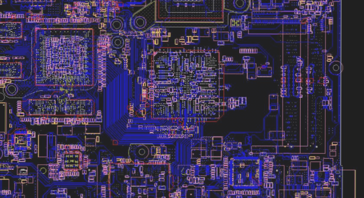
PCB technology originated in 1936, with its extensive use beginning in U.S. military radios in 1943. Since the mid-1950s, PCB technology has been widely adopted.
Today, PCBs are considered the “mother of electronic products,” with applications spanning across various sectors of the electronics industry, including computers, communications, consumer electronics, industrial control, medical equipment, defense ordnance, and aerospace.
PCBs have evolved from single-layer to double-sided, multi-layer, and flexible designs, each continuing to exhibit growth trends. The relentless push for higher precision, density, and reliability, coupled with reductions in size and cost, along with enhanced functionality, ensures that printed circuit boards will remain vital for future advancements in electronic equipment.
So, how is a PCB designed? Understanding the following seven steps will provide clarity: 1. Preliminary preparations, including the creation of component libraries and schematic diagrams. Before initiating PCB design, it’s essential to prepare the schematic (SCH) component library and PCB component packaging library.
Ideally, the PCB component packaging library should be created by the engineer based on the dimensions and materials of the selected components. The PCB component package library is generally established first, followed by the SCH component library.

1. PCB component packaging library requirements are stringent, indirectly influencing PCB installation. While SCH component library requirements are relatively flexible, precise definition of pin attributes and their correlation with the PCB component packaging library is crucial.
2. PCB layout design begins with confirming the circuit board size and machine positioning. Draw the PCB board frame and arrange connectors, buttons/switches, screw holes, and assembly holes based on positioning requirements. Consider and confirm wiring and non-wiring areas, such as the space around screw holes designated as non-wiring areas.
3. PCB structure design involves placing components within the PCB frame according to design specifications. Create a collection list (Design-Create Netlist) using the Daoli map tool and import it into the PCB software (Design-Import Netlist). Once imported, the collection list becomes part of the software background. Use the Placement operation to position all devices, visualizing connections through flying lines between pins. The PCB structure design is a critical phase, with larger boards increasing complexity and affecting previous wiring difficulty.
4. PCB wiring design is the most detailed process in PCB design, significantly impacting the board’s functionality. Wiring typically falls into three categories: distribution (basic entry-level requirement), electrical function satisfaction (a measure of PCB quality), and neatness (essential for ease of revision, testing, and maintenance). Wiring must be organized and free of clutter to avoid complications.
5. Wiring optimization and silk screen placement highlight the principle that “PCB design is an art with imperfections.” Achieving all hardware design requirements often involves trade-offs. For instance, a PCB initially designed as a 6-layer board might be modified to a 4-layer board due to cost constraints, affecting signal quality and crosstalk. Optimization usually takes twice as long as initial wiring, and after optimizing, attention must shift to silk screen placement, ensuring bottom silk screen characters are mirrored to avoid confusion with the top silk screen.
6. DRC inspection and layout inspection are key to PCB quality control. Quality control measures include self-inspection, mutual inspection, expert review meetings, and special inspections. Collecting DRC and layout examination confirms that the PCB design meets the input prerequisites of the schematic netlist and layout element diagram. Designers use checklists from company standards and personal experience. Special inspections, such as Valor and DFM inspections, focus on PCB design and output file processing.
7. Before PCB manufacturing begins, the circuit board designer must collaborate with the PCB supplier’s PE to address processing queries. This includes PCB model selection, circuit layer width adjustments, impedance control, PCB stack thickness, processing technology, aperture control, and commission standards.
Today, PCBs are considered the “mother of electronic products,” with applications spanning across various sectors of the electronics industry, including computers, communications, consumer electronics, industrial control, medical equipment, defense ordnance, and aerospace.
PCBs have evolved from single-layer to double-sided, multi-layer, and flexible designs, each continuing to exhibit growth trends. The relentless push for higher precision, density, and reliability, coupled with reductions in size and cost, along with enhanced functionality, ensures that printed circuit boards will remain vital for future advancements in electronic equipment.
So, how is a PCB designed? Understanding the following seven steps will provide clarity: 1. Preliminary preparations, including the creation of component libraries and schematic diagrams. Before initiating PCB design, it’s essential to prepare the schematic (SCH) component library and PCB component packaging library.
Ideally, the PCB component packaging library should be created by the engineer based on the dimensions and materials of the selected components. The PCB component package library is generally established first, followed by the SCH component library.

1. PCB component packaging library requirements are stringent, indirectly influencing PCB installation. While SCH component library requirements are relatively flexible, precise definition of pin attributes and their correlation with the PCB component packaging library is crucial.
2. PCB layout design begins with confirming the circuit board size and machine positioning. Draw the PCB board frame and arrange connectors, buttons/switches, screw holes, and assembly holes based on positioning requirements. Consider and confirm wiring and non-wiring areas, such as the space around screw holes designated as non-wiring areas.
3. PCB structure design involves placing components within the PCB frame according to design specifications. Create a collection list (Design-Create Netlist) using the Daoli map tool and import it into the PCB software (Design-Import Netlist). Once imported, the collection list becomes part of the software background. Use the Placement operation to position all devices, visualizing connections through flying lines between pins. The PCB structure design is a critical phase, with larger boards increasing complexity and affecting previous wiring difficulty.
4. PCB wiring design is the most detailed process in PCB design, significantly impacting the board’s functionality. Wiring typically falls into three categories: distribution (basic entry-level requirement), electrical function satisfaction (a measure of PCB quality), and neatness (essential for ease of revision, testing, and maintenance). Wiring must be organized and free of clutter to avoid complications.
5. Wiring optimization and silk screen placement highlight the principle that “PCB design is an art with imperfections.” Achieving all hardware design requirements often involves trade-offs. For instance, a PCB initially designed as a 6-layer board might be modified to a 4-layer board due to cost constraints, affecting signal quality and crosstalk. Optimization usually takes twice as long as initial wiring, and after optimizing, attention must shift to silk screen placement, ensuring bottom silk screen characters are mirrored to avoid confusion with the top silk screen.
6. DRC inspection and layout inspection are key to PCB quality control. Quality control measures include self-inspection, mutual inspection, expert review meetings, and special inspections. Collecting DRC and layout examination confirms that the PCB design meets the input prerequisites of the schematic netlist and layout element diagram. Designers use checklists from company standards and personal experience. Special inspections, such as Valor and DFM inspections, focus on PCB design and output file processing.
7. Before PCB manufacturing begins, the circuit board designer must collaborate with the PCB supplier’s PE to address processing queries. This includes PCB model selection, circuit layer width adjustments, impedance control, PCB stack thickness, processing technology, aperture control, and commission standards.

