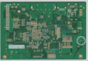
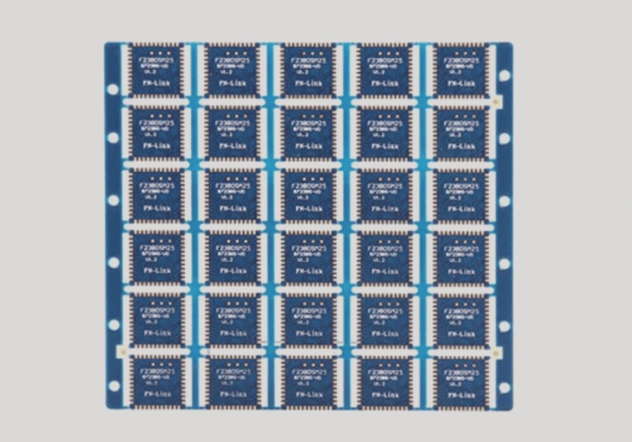
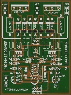
In the PCB copying process, especially when replicating high-precision circuit boards, testing is an essential step. Only through testing can we determine whether these copied PCBs meet the required standards. It is well-known that the most commonly used testing tools for circuit board duplication are the flying probe tester and test rack testing. However, there is another electronic testing device known as AOI (Automated Optical Inspection). AOI is a relatively new testing technology that has emerged in recent years but has advanced rapidly. Nowadays, many manufacturers have adopted AOI testing equipment. During the automated inspection, the system uses a camera to scan the PCB, capturing images. These images are then compared with the predefined parameters stored in the database. After processing the images, the system identifies defects on the copied PCB and highlights them on the display or uses automatic marking for technicians to address and repair the issues.
1. **Implementation Objectives:** The implementation of AOI serves two main purposes:
(1) **End Quality**: This objective focuses on monitoring the final condition of the product as it leaves the production line. It is especially important when the production issues are well-defined, product variety is high, and factors like quantity and speed are critical. AOI is typically placed at the end of the production line, where it can generate valuable process control data.
(2) **Process Tracking**: This involves using inspection equipment to monitor the production process itself. It generally provides detailed defect classification and component placement deviation information. When product reliability is paramount, low-mix, high-volume manufacturing is involved, and the supply of stable components is ensured, manufacturers prioritize this objective. In such cases, inspection equipment may be positioned at several points along the production line to monitor specific stages in real-time, providing crucial information for adjustments to the production process.
**Placement Location**: Although AOI can be used in various locations along the production line, with each position detecting specific defects, the AOI inspection equipment should be strategically placed where it can identify and correct the most defects as quickly as possible.
2. There are three key inspection stages:
(1) **After solder paste printing**. If the solder paste printing process meets the required standards, it can significantly reduce the number of defects detected by ICT. Common printing defects include:
A. Insufficient solder on the pad.
B. Excess solder on the pad.
C. Poor alignment of solder paste to the pad.
D. Solder bridges between pads.
In ICT, the likelihood of defects increases with the severity of these issues. Minor under-soldering rarely results in defects, whereas more severe cases, such as no solder at all, almost always lead to defects in ICT. Insufficient solder may result in missing components or open solder joints. However, it’s important to note that component loss can occur due to other factors as well, and these should also be considered in the inspection plan. Inspection at this stage is crucial for process monitoring and characterization. The quantitative data generated includes printing offset and solder volume, while qualitative information about the printed solder is also obtained.
(2) **Before reflow soldering**. This inspection occurs after components are placed onto the solder paste on the PCB but before the board enters the reflow oven. This is a typical inspection point for machines, as most defects from solder paste printing and component placement can be detected here. The quantitative process control data generated at this stage provides insights into the calibration of high-speed placement machines and fine-pitch component placement equipment. This data can be used to adjust component placement or to indicate when placement machines need recalibration. Inspection at this stage helps achieve effective process tracking.
(3) **After reflow soldering**. Inspection at this final stage of the SMT process is the most common use for AOI systems, as it can identify all assembly errors. Post-reflow inspection offers a high level of confidence, as it detects defects originating from solder paste printing, component placement, and the reflow process itself.
If you have any PCB manufacturing needs, please do not hesitate to contact me.Contact me