1. As a PCB expert, it is important to understand the common layer structures of PCB boards, which include single-layer boards, double-layer boards, and multi-layer boards.
2. Single-layer boards consist of a single layer of substrate material with conductive copper traces on one side, while double-layer boards have a layer of substrate material with copper traces on both sides.
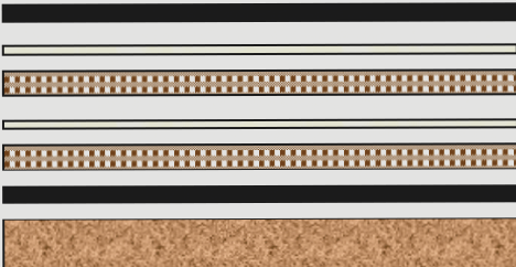
3. Multi-layer boards, on the other hand, consist of multiple layers of substrate material with copper traces interconnected through vias, allowing for more complex circuit designs and higher component density.
4. Understanding the differences and advantages of each layer structure is crucial in determining the most suitable PCB board for a specific application or design requirement.

1. Single layer board: A circuit board with only one side coated with copper and the other side not coated with copper. Usually, components are placed on the side without copper coating, which is mainly used for wiring and welding.
A single-panel is the simplest form of PCB board, with only one side covered with copper foil. A single panel is suitable for simple circuits such as electronic clocks, toys, etc. The production process of a single panel is simple and cost-effective, but its functions are relatively simple.
2. Double layer board: A circuit board with copper coated on both sides, usually referred to as the top layer on one side and the bottom layer on the other side. Generally, the top layer is used as the surface for placing components, and the bottom layer is used as the welding surface for components.
The production of double-sided panels is more complex than that of single panels, but easier to manufacture than multi-layer panels. Double-sided boards are suitable for circuits of medium complexity, such as audio, television, etc. The production of dual panels is flexible, and components can be arranged on both sides of the board.
3. Multilayer board: A circuit board containing multiple working layers, including several intermediate layers in addition to the top and bottom layers. Typically, the intermediate layer can serve as a wire layer, signal layer, power layer, grounding layer, etc. Layers are insulated from each other, and the connection between layers is usually achieved through holes.
The production of multi-layer boards is more complex than that of double panels, but it can improve the density and performance of the circuit. Multilayer boards are suitable for high-density, high-speed, and high-frequency circuits, such as computers, mobile phones, etc. Multilayer boards can increase the number of layers as needed to improve circuit performance.
Detailed introduction to PCB board layers
PCB is an indispensable part of modern electronic devices, playing a role in connecting, transmitting signals, supporting and protecting electronic components in electronic devices. PCB is usually composed of multiple layers of PCB boards, each with different functions and characteristics.
1. Signal Layer
The signal layer is the most important in the PCB board, which is the main layer connecting various components. On the signal layer, circuits, signal transmission lines, power lines, and grounding wires are usually arranged. The wiring design of the signal layer directly affects the performance and reliability of the entire PCB.
2. Power Layer
The power layer is a layer in the PCB board that is mainly used to connect the power supply and ground wire. On the power layer, power and ground wires are usually arranged to ensure a stable and reliable power supply for the entire PCB.
3. Ground Layer
The ground wire layer is also a layer in the PCB board, mainly used to connect the ground wires of various components. On the ground wire layer, grounding and power lines are usually arranged to ensure stable and reliable ground wire connections throughout the entire PCB.
4. Pad Layer
The pad layer is a layer in a PCB board that is mainly used to connect components and PCB boards. On the pad layer, pads and sockets are usually arranged to allow components to be connected to the PCB board.
5. Assembly Layer
The assembly layer is a layer in a PCB board, mainly used for assembling components. On the assembly layer, the installation positions and methods of components are usually arranged for PCB manufacturers to assemble and weld components.
6. Solder Mask Layer
The solder mask layer is a layer in the PCB board, mainly used to prevent short circuits and poor soldering during the welding process. On the solder layer, a layer of green paint is usually applied to protect the PCB board from chemical corrosion and mechanical damage.
7. Copper Layer
The copper-clad layer is a layer in a PCB board that is mainly used to provide circuit connections and support. On the copper-clad layer, circuits and signal transmission lines are usually arranged to ensure stable and reliable circuit connection of the entire PCB.
In summary, each layer of a PCB board has different functions and characteristics. In the design and manufacturing process of a PCB, it is necessary to fully consider the requirements and limitations of each layer to ensure the performance and reliability of the PCB.
When selecting a PCB design layer, the following issues should be considered
1. Purpose
Where will the PCB be used? PCB is used in various types of simple to complex electronic devices. Therefore, the first step is to clarify whether the application has minimal functionality or complex functionality.
2. Required signal type
The selection of the number of layers also depends on the type of signal they need to transmit. The signals are divided into high-frequency, low-frequency, ground or power sources. For applications that require multiple signal processing, multi-layer PCBs are required, and these circuits may require different grounding and isolation.
3. Type of through-hole
The selection of through holes is another important factor to consider. If you choose to bury through holes, more internal layers may be required, so it can meet the multi-layer requirements accordingly.
4. The density and number of required signal layers
The determination of the PCB layer is also based on two important factors: signal layer and pin density. The number of layers in a PCB increases as the pin density decreases. The pin density is 1.0. For example, a pin density of 1 would require 2 signal layers. However, pin density<0.2 may require 10 layers or more.
The efficiency of a PCB board depends on the number of layers, therefore, selecting the correct number of PCB layers is crucial.
2. Single-layer boards consist of a single layer of substrate material with conductive copper traces on one side, while double-layer boards have a layer of substrate material with copper traces on both sides.
3. Multi-layer boards, on the other hand, consist of multiple layers of substrate material with copper traces interconnected through vias, allowing for more complex circuit designs and higher component density.
4. Understanding the differences and advantages of each layer structure is crucial in determining the most suitable PCB board for a specific application or design requirement.

1. Single layer board: A circuit board with only one side coated with copper and the other side not coated with copper. Usually, components are placed on the side without copper coating, which is mainly used for wiring and welding.
A single-panel is the simplest form of PCB board, with only one side covered with copper foil. A single panel is suitable for simple circuits such as electronic clocks, toys, etc. The production process of a single panel is simple and cost-effective, but its functions are relatively simple.
2. Double layer board: A circuit board with copper coated on both sides, usually referred to as the top layer on one side and the bottom layer on the other side. Generally, the top layer is used as the surface for placing components, and the bottom layer is used as the welding surface for components.
The production of double-sided panels is more complex than that of single panels, but easier to manufacture than multi-layer panels. Double-sided boards are suitable for circuits of medium complexity, such as audio, television, etc. The production of dual panels is flexible, and components can be arranged on both sides of the board.
3. Multilayer board: A circuit board containing multiple working layers, including several intermediate layers in addition to the top and bottom layers. Typically, the intermediate layer can serve as a wire layer, signal layer, power layer, grounding layer, etc. Layers are insulated from each other, and the connection between layers is usually achieved through holes.
The production of multi-layer boards is more complex than that of double panels, but it can improve the density and performance of the circuit. Multilayer boards are suitable for high-density, high-speed, and high-frequency circuits, such as computers, mobile phones, etc. Multilayer boards can increase the number of layers as needed to improve circuit performance.
Detailed introduction to PCB board layers
PCB is an indispensable part of modern electronic devices, playing a role in connecting, transmitting signals, supporting and protecting electronic components in electronic devices. PCB is usually composed of multiple layers of PCB boards, each with different functions and characteristics.
1. Signal Layer
The signal layer is the most important in the PCB board, which is the main layer connecting various components. On the signal layer, circuits, signal transmission lines, power lines, and grounding wires are usually arranged. The wiring design of the signal layer directly affects the performance and reliability of the entire PCB.
2. Power Layer
The power layer is a layer in the PCB board that is mainly used to connect the power supply and ground wire. On the power layer, power and ground wires are usually arranged to ensure a stable and reliable power supply for the entire PCB.
3. Ground Layer
The ground wire layer is also a layer in the PCB board, mainly used to connect the ground wires of various components. On the ground wire layer, grounding and power lines are usually arranged to ensure stable and reliable ground wire connections throughout the entire PCB.
4. Pad Layer
The pad layer is a layer in a PCB board that is mainly used to connect components and PCB boards. On the pad layer, pads and sockets are usually arranged to allow components to be connected to the PCB board.
5. Assembly Layer
The assembly layer is a layer in a PCB board, mainly used for assembling components. On the assembly layer, the installation positions and methods of components are usually arranged for PCB manufacturers to assemble and weld components.
6. Solder Mask Layer
The solder mask layer is a layer in the PCB board, mainly used to prevent short circuits and poor soldering during the welding process. On the solder layer, a layer of green paint is usually applied to protect the PCB board from chemical corrosion and mechanical damage.
7. Copper Layer
The copper-clad layer is a layer in a PCB board that is mainly used to provide circuit connections and support. On the copper-clad layer, circuits and signal transmission lines are usually arranged to ensure stable and reliable circuit connection of the entire PCB.
In summary, each layer of a PCB board has different functions and characteristics. In the design and manufacturing process of a PCB, it is necessary to fully consider the requirements and limitations of each layer to ensure the performance and reliability of the PCB.
When selecting a PCB design layer, the following issues should be considered
1. Purpose
Where will the PCB be used? PCB is used in various types of simple to complex electronic devices. Therefore, the first step is to clarify whether the application has minimal functionality or complex functionality.
2. Required signal type
The selection of the number of layers also depends on the type of signal they need to transmit. The signals are divided into high-frequency, low-frequency, ground or power sources. For applications that require multiple signal processing, multi-layer PCBs are required, and these circuits may require different grounding and isolation.
3. Type of through-hole
The selection of through holes is another important factor to consider. If you choose to bury through holes, more internal layers may be required, so it can meet the multi-layer requirements accordingly.
4. The density and number of required signal layers
The determination of the PCB layer is also based on two important factors: signal layer and pin density. The number of layers in a PCB increases as the pin density decreases. The pin density is 1.0. For example, a pin density of 1 would require 2 signal layers. However, pin density<0.2 may require 10 layers or more.
The efficiency of a PCB board depends on the number of layers, therefore, selecting the correct number of PCB layers is crucial.


