1. When designing a circuit board with PCB prototyping, the circuit schematic may be well-designed or even excellent, but various types of noise can emerge during the debugging phase. As a result, the circuit board may fail to meet the expected performance, and sometimes, the board will need to be remade.
2. So, how can we reduce PCB noise? Let’s break it down. For a well-designed circuit board, experienced electronic engineers can quickly assess its general layout (as long as they understand the board’s intended functionality). This is based on the principle of functional module separation. Each functional module consists of multiple electronic components that work together to perform specific tasks within the circuit. In practice, we aim to place these components as close together as possible to minimize the length of the traces, thereby enhancing the performance of the module.
3. It’s not difficult to see this principle in action with common development boards or mobile phones, especially the latter. If you disassemble a mobile phone, you will notice a clear separation between modules, each of which is shielded by a Faraday cage to minimize noise and interference.

**How to Reduce Noise on the Circuit Board**
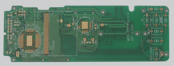
The development board shown above is a PCB. From the layout, it is clear that the interface circuits are well separated, and the routing of SDRAM, DDR, and SD card interface circuits is designed to avoid mutual interference.
By dividing the system into distinct modules, signal integrity is enhanced, high-frequency interference between modules is minimized, and overall system stability is improved. Additionally, when both analog and digital circuits are present on the same PCB, it is crucial to physically separate these two types of circuits. If separation is not possible, a “silent area” should be created. A silent area is a designated space where analog and digital circuits or functional modules are kept apart. This isolation helps prevent interference from one module affecting another. In the PCB example above, the silent zone is clearly visible.
It is important to note that the silent area should not be connected to the ground of the circuit board.
In actual PCB prototyping, not every design has the luxury of ample space to create a silent area. So, what should be done when space is limited? Here are a few solutions:
A. **Use Transformers or Signal Isolation Components**
This approach involves using components such as CMOS devices or transistors to create separation in the circuit. This ensures that signals are isolated, preventing interference between sensitive analog and noisy digital circuits.
B. **Filter Signals Before Entering the Module**
This method, commonly used to prevent Electrostatic Discharge (ESD), also helps in reducing high-frequency and high-voltage noise. A well-designed filter can effectively block noise and protect the integrity of the signal.
C. **Use Common-Mode Inductors for Signal Protection**
Common-mode inductors play a key role in stabilizing signals and reducing noise interference. While they may appear as simple inductive components in a schematic, their impact on signal integrity and noise suppression is significant.
On the other hand, PCB prototyping also highlights that electronic engineers need considerable experience to refine their designs. A design technique similar to creating a silent area is **trench protection technology**. This method involves removing copper from a specific area (the silent zone) to expose the base PCB material, which acts as a shield. The concept of “bridges” arises here: these are the power, ground, and signal lines connecting different parts of the circuit.
Trench technology is effective in withstanding peak voltages and improving discharge protection, which, to some extent, can help in reducing circuit board noise.
In PCB design, care must be taken to avoid routing signals through trenches that are unrelated to the isolation areas, as this can lead to the generation of RF loop currents, which may degrade the performance of the board. It’s also important to note that many analog-to-digital and digital-to-analog components are often connected to a shared ground. For example, ADC and DAC devices should be isolated, with a clear reference ground to prevent noise and EMI. If the digital signal current cannot effectively return to the ground source, noise will be generated.
When designing the schematic, we find that properly segregating **AGND** and **DGND** pins can greatly improve performance, making the design process easier. Typically, PCB prototyping involves partitioning the circuit into functional modules and designing distinct static areas between these partitions. This helps to minimize the influence of power and ground on the signals, ultimately reducing the noise on the circuit board.
If your have any questions about PCB ,please contact me info@wellcircuits.com
2. So, how can we reduce PCB noise? Let’s break it down. For a well-designed circuit board, experienced electronic engineers can quickly assess its general layout (as long as they understand the board’s intended functionality). This is based on the principle of functional module separation. Each functional module consists of multiple electronic components that work together to perform specific tasks within the circuit. In practice, we aim to place these components as close together as possible to minimize the length of the traces, thereby enhancing the performance of the module.
3. It’s not difficult to see this principle in action with common development boards or mobile phones, especially the latter. If you disassemble a mobile phone, you will notice a clear separation between modules, each of which is shielded by a Faraday cage to minimize noise and interference.

**How to Reduce Noise on the Circuit Board**
The development board shown above is a PCB. From the layout, it is clear that the interface circuits are well separated, and the routing of SDRAM, DDR, and SD card interface circuits is designed to avoid mutual interference.
By dividing the system into distinct modules, signal integrity is enhanced, high-frequency interference between modules is minimized, and overall system stability is improved. Additionally, when both analog and digital circuits are present on the same PCB, it is crucial to physically separate these two types of circuits. If separation is not possible, a “silent area” should be created. A silent area is a designated space where analog and digital circuits or functional modules are kept apart. This isolation helps prevent interference from one module affecting another. In the PCB example above, the silent zone is clearly visible.
It is important to note that the silent area should not be connected to the ground of the circuit board.
In actual PCB prototyping, not every design has the luxury of ample space to create a silent area. So, what should be done when space is limited? Here are a few solutions:
A. **Use Transformers or Signal Isolation Components**
This approach involves using components such as CMOS devices or transistors to create separation in the circuit. This ensures that signals are isolated, preventing interference between sensitive analog and noisy digital circuits.
B. **Filter Signals Before Entering the Module**
This method, commonly used to prevent Electrostatic Discharge (ESD), also helps in reducing high-frequency and high-voltage noise. A well-designed filter can effectively block noise and protect the integrity of the signal.
C. **Use Common-Mode Inductors for Signal Protection**
Common-mode inductors play a key role in stabilizing signals and reducing noise interference. While they may appear as simple inductive components in a schematic, their impact on signal integrity and noise suppression is significant.
On the other hand, PCB prototyping also highlights that electronic engineers need considerable experience to refine their designs. A design technique similar to creating a silent area is **trench protection technology**. This method involves removing copper from a specific area (the silent zone) to expose the base PCB material, which acts as a shield. The concept of “bridges” arises here: these are the power, ground, and signal lines connecting different parts of the circuit.
Trench technology is effective in withstanding peak voltages and improving discharge protection, which, to some extent, can help in reducing circuit board noise.
In PCB design, care must be taken to avoid routing signals through trenches that are unrelated to the isolation areas, as this can lead to the generation of RF loop currents, which may degrade the performance of the board. It’s also important to note that many analog-to-digital and digital-to-analog components are often connected to a shared ground. For example, ADC and DAC devices should be isolated, with a clear reference ground to prevent noise and EMI. If the digital signal current cannot effectively return to the ground source, noise will be generated.
When designing the schematic, we find that properly segregating **AGND** and **DGND** pins can greatly improve performance, making the design process easier. Typically, PCB prototyping involves partitioning the circuit into functional modules and designing distinct static areas between these partitions. This helps to minimize the influence of power and ground on the signals, ultimately reducing the noise on the circuit board.
If your have any questions about PCB ,please contact me info@wellcircuits.com


